w w .vvv i hi uiu, : ii iva ;j « ili.^.a i.lw.u m-fcjvv i...
TRANSCRIPT
W ... w .VvVj i Hi, U iU: ii i v a ; « ili.^.A i.lW.U A ? t-t - . - : i <rfc Jir- T« « h
m-fcjvv i ^ i s
»-At ' ' : • '-iJ
l>Lfcj I p V E f t S i t i : i f i ® v i 0 5 ! i u i i r M S f c t S © M

PERPUSTAKAAN UTHM
' 3 0 0 0 0 0 0 1 8 8 3 6 1 6 '
KOLEJ UNIVERSITI TEKNOLOGI TUN HUSSEIN ONN
PENGESAHAN STATUS LAPORAN PROJEK SARJANA
SIMULATION, FABRICATION AND CHARACTERIZATION OF
NMOS TRANSISTOR
SESI PENGAJIAN : 2006/2007
Saya DAMHUJ1 BIN RIFAI mengaku membenarkan Laporan Projek Sarjana ini disimpan di Perpustakaan dengan syarat-syarat kegunaan seperti berikut:
1. 2.
3.
4.
Laporan Projek Sarjana adalah hakmilik Kolej Universiti Teknologi Tun Hussein Onn. Perpustakaan dibenarkan membuat salinan untuk tujuan pengajian sahaja. Perpustakaan dibenarkan membuat salinan tesis ini sebagai bahan pertukaran antara institusi pengajian tinggi. ** Sila tandakan (V)
SULIT
TERHAD
TIDAK TERHAD
(Mengandungi maklumat yang berdaijah keselamatan atau kepentingan Malaysia seperti yang termaktub di dalam AKTA RAHSIA RASMI 1972)
(Mengandungi maklumat TERHAD yang telah ditentukan oleh organisasi/badan di mana penyelidikan dijalankan
Disahkan oleh
(TANDATANGAN PENULIS)
Alamat Tetap:
12, LOT 392, JALAN TENGAH 7,
BATU 6 '/2 GOMBAK,
53100, GOMBAK SELANGOR.
(TANI^TANGWPENYELIA)
PROFESSOR DR. HASHIM BIN SAIM
Nama Penyelia
Tarikh: 21 DISEMBER 2006 Tarikh: 21 DISEMBER 2006
CATATAN: ** Jika Laporan Projek Saijana ini SULIT atau TERHAD, sila lampirkan surat
daripada pihak berkuasa/organisasi berkenaan dengan menyatakan sekali sebab dan tempoh laporan ini perlu di kelaskan sebagai SULIT atau TERHAD.
" I hereby declare that I have read this thesis and in my opinion this thesis in terms of
content and quality requirement fulfills the purpose for the award of the Master of
Electrical Engineering"
Signature
Name of Supervisor
Date
: PROF. Dr. HASHIM BIN SAIM
: 21 DECEMBER 2006
SIMULATION, FABRICATION AND CHARACTERIZATION OF NMOS
TRANSISTOR
DAMHUJI B. RIFAI
This thesis is submitted in partial to fulfillment of the requirement for the
Master of Electrical Engineering
Faculty of Electrical And Electronic Engineering
Tun Hussien Onn University College of Technology
DECEMBER, 2006
ii
" I hereby declare that the work in this thesis in my own except for quotations and
summaries which have been duly acknowledged"
Signature : -.
Name of Student : DAMHUJI BIN RIFAI
Date : 21 DECEMBER 2006
iii
To my parents; for your love and support
IV
ACKNOWLEDGEMENTS
All praises be to Allah SWT. Without His hidayah, 'inayah and ri 'ayah, the
study would not come to completion. Peace and blessings be upon the beloved
Prophet SAW, with his Risalah and teaching the study has become meaningful to
me.
I express my gratitude and thanks from the deepest of my heart to Professor
Dr. Hashim Saim for his wonderful, resourceful and enlightening supervision. His
wisdom, patient and support have been the courage and motivation of my
challenging and tiring work.
To Mohd Zainizan Sahdan, I would like to express my utmost appreciation
for his strong commitment in assisting me for the eventual completion of my work.
Many thanks I dedicate to technician in KUiTTHO Microfabrication
Cleanroom , Ramlan bin Ralim for his lovely cooperation in my various laboratory
tasks. I also would like to appreciate all my friends and colleagues in KUiTTHO for
the friendship and the sincere cooperation.
Lastly but not least, I would like to express my great thanks to those who
have contributed directly or indirectly in the completion of my studies. I should
admit and submit that the completion of this study owes to the contributions from all
the parties above regardless of any forms.
IV
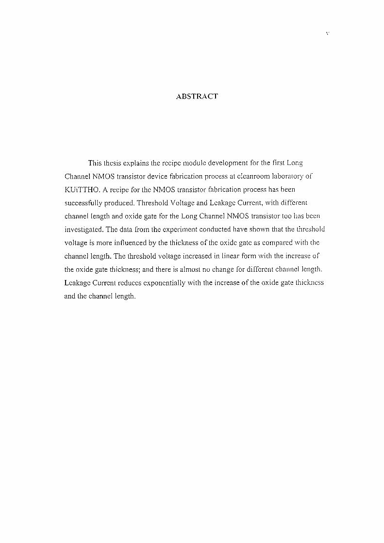
ABSTRACT
This thesis explains the recipe module development for the first Long
Channel NMOS transistor device fabrication process at cleanroom laboratory of
KUiTTHO. A recipe for the NMOS transistor fabrication process has been
successfully produced. Threshold Voltage and Leakage Current, with different
channel length and oxide gate for the Long Channel NMOS transistor too has been
investigated. The data from the experiment conducted have shown that the threshold
voltage is more influenced by the thickness of the oxide gate as compared with the
channel length. The threshold voltage increased in linear form with the increase of
the oxide gate thickness; and there is almost no change for different channel length.
Leakage Current reduces exponentially with the increase of the oxide gate thickness
and the channel length.
IV
ABSTRAK
Tesis ini menerangkan pembangunan modul resepi bagi proses fabrikasi
peranti transistor kesan medan logam-oksida semikonduktor salur panjang {Long
Channel NMOS transistor) yang pertama kali di makmal bilik bersih KUiTTHO.
Resepi bagi proses fabrikasi peranti transistor kesan medan logam-oksida
semikonduktor telah berjaya dihasilkan. Voltan ambang dan arus bocor salir, dengan
panjang salur dan oksida get yang berbeza bagi transistor kesan medan logam-oksida
semikonduktor salur panjang telah di kaji. Data dari eksperimen yang telah dilakukan
menunjukkan voltan ambang banyak di pengaruhi oleh ketebalan oksida get
berbanding dengan panjang salur. Voltan ambang naik secara linear dengan kenaikan
ketebalan oksida get dan hampir tidak ada perubahan bagi panjang salur yang
berbeza. Arus bocor salir berkurangan secara eksponen dengan kenaikan ketebalan
oksida get dan panjang salur.

vii
CONTENTS
CHAPTER TITLE PAGE
TITLE i
DECLARATION ii
DEDICATION iii
ACKNOWLEDGEMENT iv
ABSTRACK v
ABSTRAK vi
TABLE OF CONTENT vii
LIST OF TABLES xi
LIST OF FIGURES xii
LIST OF SYMBOLS xvii
LIST OF APPENDIX xx
I PROJECT OVERVIEW 1
1.1 Overview 1
1.2 Introduction - 1
1.3 Problem Aspire 4
1.4 Objectives 4
1.5 Project Scope 5
Vlll
II LITERATURE REVIEW - MOS TRANSISTOR 6
2.1 Introduction 6
2.2 The MOS Transistor 9
2.2.1 The NMOS Transistor 10
2.2.2 The PMOS Transistor 12
2.3 Electrical Characteristics Of The MOS Transistor 13
2.3.1 The MOS System under External Biased
Voltage. 13
2.3.2 The MOSFET Operation 15
2.4 Fabrication process 23
2.4.1 Lithography 23
2.4.1.1 The Wafer with the substrate
Film 24
2.4.1.2 Photo Resist Deposition 24
2.4.1.3 Softbake 25
2.4.1.4 The Mask Alignment 26
2.4.1.5 Ultra Violet Radiation Exposure 26
2.4.1.6 Development 26
2.4.1.7 Photoresist strip 26
2.4.2 Diffusion 27
2.4.3 Ion Implantation 30
2.4.4 Metallization 32
2.4.5 Deposition 33
2.4.5.1 Silicon Dioxide Deposition 34
2.4.6 Etching 35
2.4.6.1 Wet etching 36
III NMOS TRANSISTOR SIMULATION 37
3.1 Overview 37
ix
3.2 NMOS Transistor Simulation 37
3.3 Linux Operating System 38
3.4 Integrated System Engineering Technology
Computer Aided Design (ISE TCAD) 3 8
3.4.1 GENESISe 41
3.4.2 Ligament Flow Editor 42
3.4.3 Ligament Layout Editor 43
3.4.4 Floops-Ise 44
3.4.5 Dessis Programming Code 46
3.4.6 Tecplot-ISE 49
3.4.7 Inspect 50
IV CLEANROOM 53
4.1 Overview 53
4.2 KUiTTHO Microfabrication Cleanroom 53
4.3 Water Purification System 56
4.4 Equipment Process 58
4.4.1 Oxidation and Diffusion furnace 58
4.4.2 Photolithography module 61
4.4.3 Wet Etching Modules 64
4.4.4 Wafer Test Module 65
4.4.5 Consumable 68
V THE FABRICATION PROCESS OF NMOS
TRANSISTOR 69
5.1 Overview 69
5.2 Preliminary research 69
5.2.1 Dry oxidation 70
5.2.3 Wet oxidation 71
IV
5.2.4 Aluminum Deposition 73
5.3 Mask Design 74
5.4 Fabrication Process of NMOS Transistor 77
VI RESULT AND DISCUSSION 87
6.1 Overview 87
6.2 NMOS transistor Simulation 87
6.2.1 Channel length effect 88
6.2.2 Oxide gate thickness effect 93
6.3 NMOS Transistor Fabrication 97
6.3.1 Preliminary Research 97
6.3.2 Fabrication Process 100
VII CONCLUSION 112
7.1 Overview 112
7.2 Conclusion 114
7.3 Problem 113
7.4 Future suggestion 114
REFERENCES 116
xi
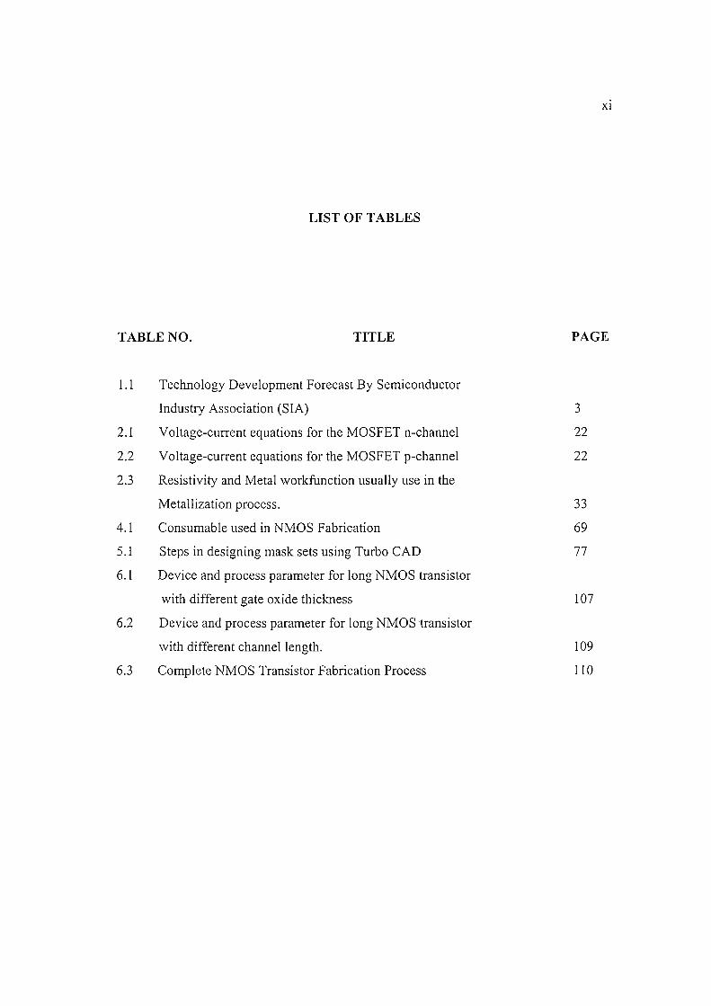
LIST OF TABLES
TABLE NO. TITLE PAGE
1.1 Technology Development Forecast By Semiconductor
Industry Association (SIA) 3
2.1 Voltage-current equations for the MOSFET n-channel 22
2.2 Voltage-current equations for the MOSFET p-channel 22
2.3 Resistivity and Metal workfunction usually use in the
Metallization process. 33
4.1 Consumable used in NMOS Fabrication 69
5.1 Steps in designing mask sets using Turbo CAD 77
6.1 Device and process parameter for long NMOS transistor
with different gate oxide thickness 107
6.2 Device and process parameter for long NMOS transistor
with different channel length. 109
6.3 Complete NMOS Transistor Fabrication Process 110
Xll l
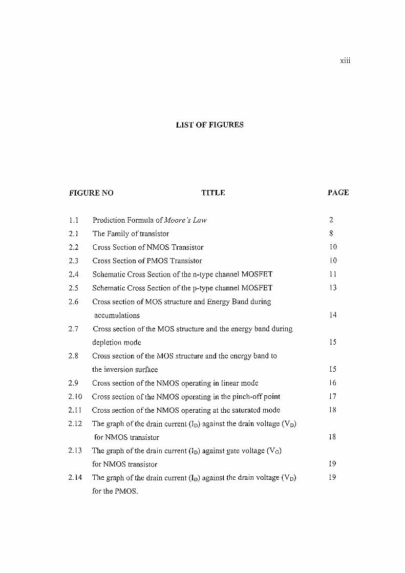
LIST OF FIGURES
FIGURE NO TITLE PAGE
1.1 Prediction Formula of Moore's Law 2
2.1 The Family of transistor 8
2.2 Cross Section of NMOS Transistor 10
2.3 Cross Section of PMOS Transistor 10
2.4 Schematic Cross Section of the n-type channel MOSFET 11
2.5 Schematic Cross Section of the p-type channel MOSFET 13
2.6 Cross section of MOS structure and Energy Band during
accumulations 14
2.7 Cross section of the MOS structure and the energy band during
depletion mode 15
2.8 Cross section of the MOS structure and the energy band to
the inversion surface 15
2.9 Cross section of the NMOS operating in linear mode 16
2.10 Cross section of the NMOS operating in the pinch-off point 17
2.11 Cross section of the NMOS operating at the saturated mode 18
2.12 The graph of the drain current (ID) against the drain voltage (VD)
for NMOS transistor 18
2.13 The graph of the drain current (ID) against gate voltage (VG)
for NMOS transistor 19
2.14 The graph of the drain current (ID) against the drain voltage (VD) 19
for the PMOS.
2.15 The graph of the drain current (ID) against the gate voltage (VG)
for the PMOS. 20
2.16 Current-voltage characteristics of the MOS transistors
n-channel including the effect of the length channel modulation 21
2.17 Patterns Transferring on the Wafer 24
2.18 Positive and negative photoresist 25
2.19 Ion distribution towards distance from the surface. 21
3.1 Process of NMOS transistor simulation using ISETC AD 41
3.2 GENESISe Window 42
3.3 Ligament Flow Editor window. 43
3.4 Ligament Layout Editor Window 45
3.5 Channel length of NMOS transistor to be developed 46
3.6 Tecplot-ISE window 51
3.7 INSPECT Window 52
3.8 Steps for obtaining the treshold voltage 53
3.8 Steps for obtaining the drain leakage current. 53
4.1 The Micro fabrication cleanroom layout,KUITTHO 55
4.2 Front view of micro fabrication cleanroom 56
4.3 View inside micro fabrication cleanroom 56
4.4 Water purification system,KUITTHO 58
4.5 Deionised water purification equipment 58
4.6 Switches Panel for Furnace Exhaust 61
4.7 Furnace Heat Exhaust System 61
4.8 Furnace Control Panel 62
4.9 The Programmable spin coater 63
4.10 The Aligner and Exposure system. 63
4.11 The Hot plate 64
4.12 Waste container and vacuum pump. 64
4.13 Wet etching module controller 65
4.14 The Spin dryer 66
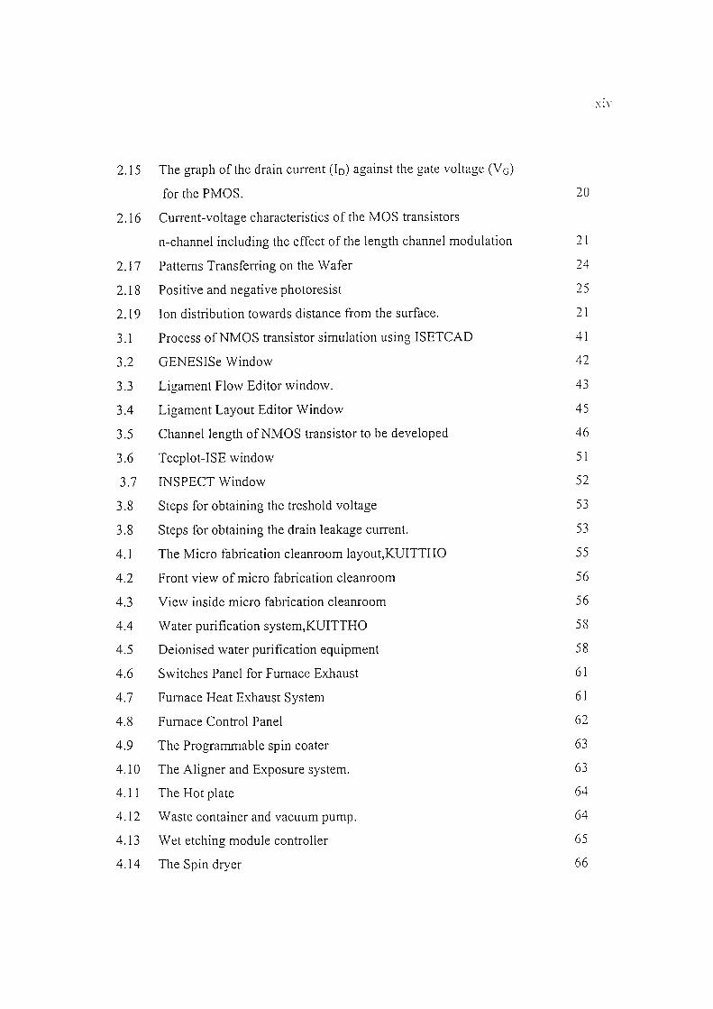
IV
4.15 The Wafer test system 67
4.16 The Capacitance measurement system 68
4.17 The 4-Point Probe 68
4.18 The H-150 Microprobe Station 69
5.1 Source/drain and gate masks 78
5.2 Contact and Metal masks 78
5.3 P-type Si wafer 81
5.4 Oxide Grown 81
5.5 Photoresist Applied 82
5.6 Photoresist Developed 82
5.7 Etch windows 82
5.8 Strip the resists with Acetone 83
5.9 N-type diffusion for P-type substrate 83
5.10 Wet Oxidation (2500A) 83
5.11 Photolithography for 2nd photo mask (gate) 84
5.12 Photoresist Developed 84
5.13 Etch Windows for Gate 84
5.14 Dry Oxidation for Gate 85
5.15 Photolithography for 3rd photo mask (Contact) 85
5.16 Photoresist Developed 85
5.17 Etch Windows for Contacts 86
5.18 Photoresist Removed 86
5.19 Metal Deposition 86
5.20 Photoresist Applied 87
5.21 Photoresist Developed 87
5.22 Etch Metal 87
5.23 Completion ofNMOS Fabrication 88
6.1 Graph of VTHgm vs. channel length 90
6.2 Graph of VTHlin vs. channel length 91
6.3 Graph of drain leakage current vs. channel length 91
6.4 IDVD characteristics o fNMOS transistor with different channel
xix
length (Tox = 2.2 nm, VG = 1 .OV} 92
6.5 IDVG characteristics o f N M O S transistor at HIGH VDS with
different channel length 93
6.6 Log IDVg characteristic at HIGH VDs o f N M O S transistor with
different channel length 93
6.7 NMOST transistor mesh profile with different channel length 94
6.8 NMOST transistor phosphorus doping profile with different
channel length 95
6.9 Graph o f V T H g m v s Gate Oxide Thickness 96
6.10 Graph o fVTHl invs Gate Oxide Thickness 96
6.11 Graph of drain leakage current vs. gate oxide thickness 97
6.12 IDVD characteristics o f N M O S transistor (L= 5 um, Tox = 1.8 nm,
VG = 1.0V) 97
6.13 IDVd characteristics o f N M O S transistor (L=5um, Tox = 1.6 nm,
VG = 1.0V) 98
6.14 IDVG characteristics o f N M O S transistor at HIGH VDS (L=5 um,
Tox = 1.8 nm) 98
6.15 IDVG characteristics of NMOS transistor at HIGH VDS (L=5 um,
Tox = 1.6 nm) 99
6.16 The growth rates of silicon oxide for dry oxidation process 100
6.17 The growth rates of silicon oxide for wet oxidation process 101
6.18 Graph of aluminium vs. size of aluminium 102
6.19 The inspection outcome in source/drain masking 103
6.20 The inspection outcome in gate masking process 103
6.21 The inspection outcome in contact masking process 104
6.22 The inspection outcome in metal masking process 104
6.23 IDVD characteristics of Long Channel NMOS transistor.
(VDS=5V, L=320um, Tox=720A) 105
6.24 IDVD characteristics of Long channel NMOS transistor
. (Vd s=5V, L=290um, Tox = 650A) 106
6.25 IDVD characteristics of Long Channel NMOS transistor.
(Vd s=5V, L= 160um, Tox=650)
IDVd characteristics of Long Channel NMOS transistor
(VDS=5V, L=270um, Tox=650A)
LIST OF SYMBOLS
A Area
A Symbol for 10"10cm or 10"8m
c Speed of light in vacuum
C Capacitance
Cj Junction capacitance per unit area
C0X Oxide capacitance per unit area
D Diffusion coefficient
E Electric field
Ea Acceptor energy
Ec Conduction band energy of a semiconductor
Ed Donor energy
Ef Fermi energy (thermal equilibrium)
E8 Energy bandgap of a semiconductor
Ei Intrinsic Fermi energy Joule
Ev Valence band energy of a semiconductor
Fn Quasi-Fermi energy of electrons
FP Quasi-Fermi energy of holes
h Plank's constant
I Current
J Current density
Jn Electron current density
Jp Hole current density
k Boltzmann's constant
XV l l l
L Length
m Mass
n Electron density
rii Intrinsic carrier density
N Doping density
Na Acceptor doping density
Nc Effective density of states in the conduction band
Nd Donor doping density
0 Charge
OP,B Hole charge in the base
Qd Charge density per unit area in the depletion layer of an MOS structure
Qdj Charge density per unit area at threshold in the depletion layer of an MOS
structure
R Resistance
t Thickness
tox Oxide thickness
T Temperature
v Velocity
v,h Thermal velocity
Va Applied voltage
VB Base voltage
VD Drain voltage
VG Body voltage
VG Gate voltage
Vt Thermal voltage
VTH Threshold voltage
xd Depletion layer width
xd, T Depletion layer width in an MOS structure at threshold
Xj Junction depth
x„ Depletion layer width in an n-type semiconductor
xp Depletion layer width in a p-type semiconductor
xix
£ox Dielectric constant of the oxide F/m
Ss Dielectric constant of the semiconductor F/m
fjn Electron mobility
fjp Hole mobility
<PM Workfunction of a metal V
&MS Workfunction difference between a metal and a semiconductor V
CHAPTER I
PROJECT OVERVIEW
1.1 Overview
This chapter will explain the project overview and scopes of project.
1.2 Introduction
The history of microelectronics began on December 1947 at the Bell Labs,
United States of America, when three scientists John Brdeen, Wafter Brattain and
William Shockley invented the first semiconductor device which is called the transistor
that was able to replace the functions of the vacuum tube as an amplifier. The said
invention had opened the path in producing electronic circuitry designs that were small
and cheap. Entailing the discovery, large numbers of electronics companies were
incorporated including one by William Shockley himself in the year 1955 in Santa Clara