modeling mosfets by using c++ - ir.unimas.my mosfets by using c++ (24 pgs).pdf · fungsi-fungsi...
TRANSCRIPT
i
Modeling MOSFETs by Using C++
ROY STEPHEN ANAK JOEL JIMBAI
This project is submitted in partial fulfilment of
The requirements for the degree of Bachelor of Engineering with Honours
(Electronic and Telecommunication Engineering)
Faculty of Engineering
UNIVERSITI MALAYSIA SARAWAK
2008/2009
UNIVERSITI MALAYSIA SARAWAK
R13a
BORANG PENGESAHAN STATUS TESIS
Judul: MODELING MOSFETs BY USING C++
SESI PENGAJIAN: 2008/2009
Saya ROY STEPHEN ANAK JOEL JIMBAI
(HURUF BESAR)
mengaku membenarkan tesis * ini disimpan di Pusat Khidmat Maklumat Akademik, Universiti Malaysia Sarawak
dengan syarat-syarat kegunaan seperti berikut:
1. Tesis adalah hakmilik Universiti Malaysia Sarawak.
2. Pusat Khidmat Maklumat Akademik, Universiti Malaysia Sarawak dibenarkan membuat salinan untuk
tujuan pengajian sahaja.
3. Membuat pendigitan untuk membangunkan Pangkalan Data Kandungan Tempatan.
4. Pusat Khidmat Maklumat Akademik, Universiti Malaysia Sarawak dibenarkan membuat salinan tesis ini
sebagai bahan pertukaran antara institusi pengajian tinggi.
5. ** Sila tandakan ( ) di kotak yang berkenaan
SULIT (Mengandungi maklumat yang berdarjah keselamatan atau kepentingan
Malaysia seperti yang termaktub di dalam AKTA RAHSIA RASMI 1972).
TERHAD (Mengandungi maklumat TERHAD yang telah ditentukan oleh organisasi/
badan di mana penyelidikan dijalankan).
TIDAK TERHAD
Disahkan oleh
(TANDATANGAN PENULIS) (TANDATANGAN PENYELIA)
Alamat tetap: 52 A, KPG QUOP BATU 10,
JLN KCH/SERIAN, 93250 KUCHING. MR. NORHUZAIMIN JULAI
Nama Penyelia
Tarikh: Tarikh:
CATATAN * Tesis dimaksudkan sebagai tesis bagi Ijazah Doktor Falsafah, Sarjana dan Sarjana Muda.
** Jika tesis ini SULIT atau TERHAD, sila lampirkan surat daripada pihak berkuasa/organisasi
berkenaan dengan menyatakan sekali sebab dan tempoh tesis ini perlu dikelaskan sebagai
SULIT dan TERHAD.

This Final Year Project attached here:
Title : Modeling MOSFETs by Using C++
Student Name : Roy Stephen anak Joel Jimbai
Matric No : 10916
has been read and approved by:
____________________ _________________
Mr. Norhuzaimin Julai Date
(Supervisor)

ii
Dedicated to my beloved family and friends

iii
ACKNOWLEDGEMENT
Upon completion of this project, I would like to express the highest appreciation
to my supervisor, Mr Norhuzaimin Julai for his endless hours of help, suggestions, ideas
and guidance during the development of this final year project.
I also would like to take the opportunity to express my gratitude to all lectures and
staffs, who helped by giving their time and guide, advice and support in the process of
making this project.
I also would like to thank my parent, Joel Jimbai and Menggusi Raeg, my family
and friends for all their love, care support and companion that helped me in sailing
through the many hard days in lives and studies all these while.
Last but not least, I would like to thank his beloved Jeascye, for her love, constant
support and understanding.
iv
ABSTRAK
Dewasa ini, penggunaan secara meluas transistor ‘Metal Oxide Semiconductor
Field-Effect Transistor’ (MOSFET) meliputi penggunaan di dalam peranti –peranti
elektronik , terutama dalam bidang rekacipta litar paduan (ICs), merupakan litar-litar
mikro yang dipasang di atas sekeping cip silikon. Oleh kerana itu, dalam laporan ini,
serba sedikit kriteria “MOSFET” dihuraikan, yang merupakan salah satu objektif untuk
projek ini iaitu untuk memodelkan kriteria-kriteria ini menggunakan sebuah perisian
yang dikenali sebagai “Microsoft Visual C++”. Fungsi-fungsi “C++” yang dihasilkan
oleh penulis sendiri, yang mana akan digunakan sebagai aplikasi untuk membuat fungsi
penyongsang (inverter), dan kemudiannya digunakan pula untuk membuktikan
penyongsangan pasangan logik-logik seperti DAN/TAKDAN, ATAU/TAKATAU dan
EKSKLUSIF ATAU/ EKSKLUSIF TAKATAU dan juga “Half-Adder”. Masalah-
masalah yang dihadapi penulis disertakan dengan pandangan dan cadangan yang
mungkin berguna untuk perintis masa depan bagi projek ini.
v
ABSTRACT
The Metal Oxide Semiconductor Field-Effect Transistors (MOSFET) has
become by far the most widely used electronic devices, especially in the design of
integrated circuits (ICs), which are circuits fabricated on a single silicon chip. The
reason for the label metal-oxide-semiconductor FET is: metal for the drains source and
gate connection to the proper surface- in particular, the gate terminal and the control to
be offered by the surface are of the contact, structure on which the n- and p-type regions
are diffused. Thus, in this paper, the characteristics of the MOSFETs are briefly
discussed at which one of the objectives is to model these characteristics by using
software, Microsoft Visual C++ and in this project, the drain characteristics of both
NMOS and PMOS is modelled. As goes further this paper, the created C++
programming for the inverter which are then further implement to verify the operation
of pairs of gate logics ; AND/NAND, OR/NOR and XOR/XNOR and also Half -Adder.
Nevertheless, the constraints faced by the author are concluded and few
recommendations are suggested for future apprentices.
vi
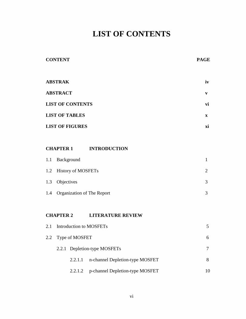
LIST OF CONTENTS
CONTENT PAGE
ABSTRAK iv
ABSTRACT v
LIST OF CONTENTS vi
LIST OF TABLES x
LIST OF FIGURES xi
CHAPTER 1 INTRODUCTION
1.1 Background 1
1.2 History of MOSFETs 2
1.3 Objectives 3
1.4 Organization of The Report 3
CHAPTER 2 LITERATURE REVIEW
2.1 Introduction to MOSFETs 5
2.2 Type of MOSFET 6
2.2.1 Depletion-type MOSFETs 7
2.2.1.1 n-channel Depletion-type MOSFET 8
2.2.1.2 p-channel Depletion-type MOSFET 10
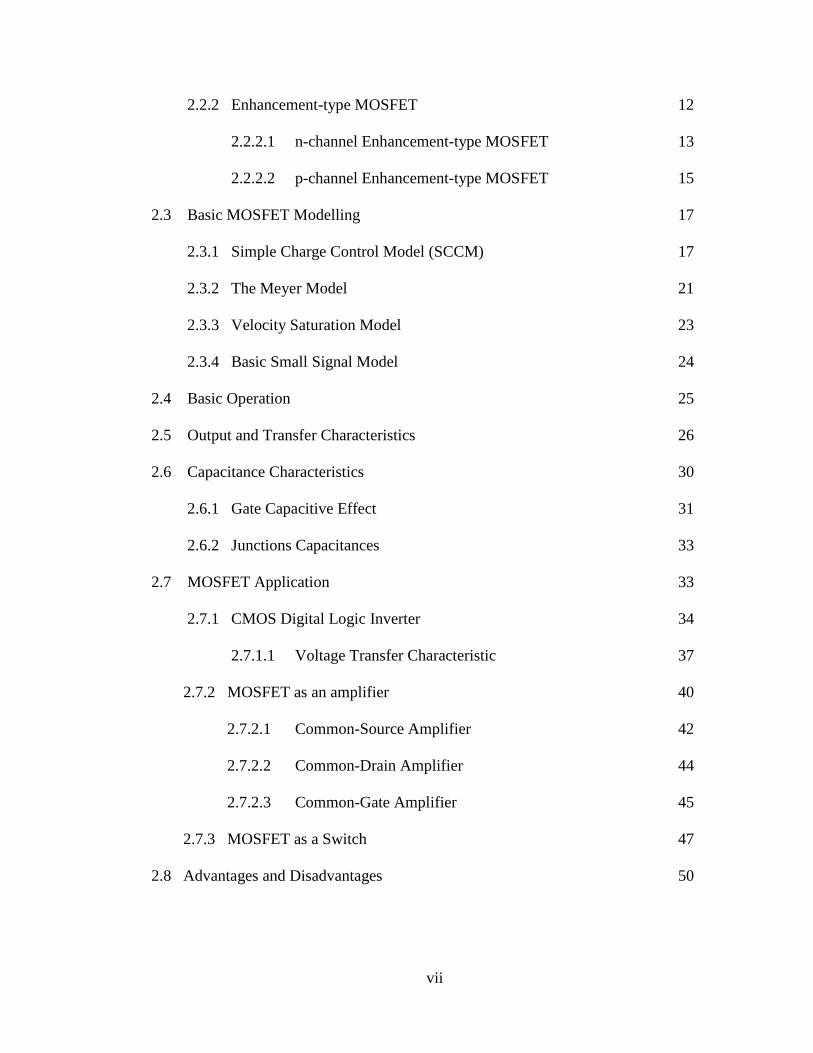
vii
2.2.2 Enhancement-type MOSFET 12
2.2.2.1 n-channel Enhancement-type MOSFET 13
2.2.2.2 p-channel Enhancement-type MOSFET 15
2.3 Basic MOSFET Modelling 17
2.3.1 Simple Charge Control Model (SCCM) 17
2.3.2 The Meyer Model 21
2.3.3 Velocity Saturation Model 23
2.3.4 Basic Small Signal Model 24
2.4 Basic Operation 25
2.5 Output and Transfer Characteristics 26
2.6 Capacitance Characteristics 30
2.6.1 Gate Capacitive Effect 31
2.6.2 Junctions Capacitances 33
2.7 MOSFET Application 33
2.7.1 CMOS Digital Logic Inverter 34
2.7.1.1 Voltage Transfer Characteristic 37
2.7.2 MOSFET as an amplifier 40
2.7.2.1 Common-Source Amplifier 42
2.7.2.2 Common-Drain Amplifier 44
2.7.2.3 Common-Gate Amplifier 45
2.7.3 MOSFET as a Switch 47
2.8 Advantages and Disadvantages 50
viii
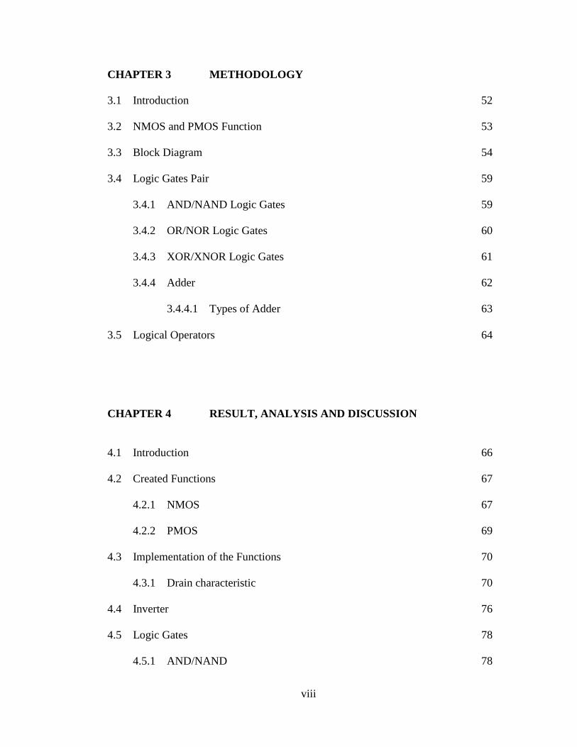
CHAPTER 3 METHODOLOGY
3.1 Introduction 52
3.2 NMOS and PMOS Function 53
3.3 Block Diagram 54
3.4 Logic Gates Pair 59
3.4.1 AND/NAND Logic Gates 59
3.4.2 OR/NOR Logic Gates 60
3.4.3 XOR/XNOR Logic Gates 61
3.4.4 Adder 62
3.4.4.1 Types of Adder 63
3.5 Logical Operators 64
CHAPTER 4 RESULT, ANALYSIS AND DISCUSSION
4.1 Introduction 66
4.2 Created Functions 67
4.2.1 NMOS 67
4.2.2 PMOS 69
4.3 Implementation of the Functions 70
4.3.1 Drain characteristic 70
4.4 Inverter 76
4.5 Logic Gates 78
4.5.1 AND/NAND 78
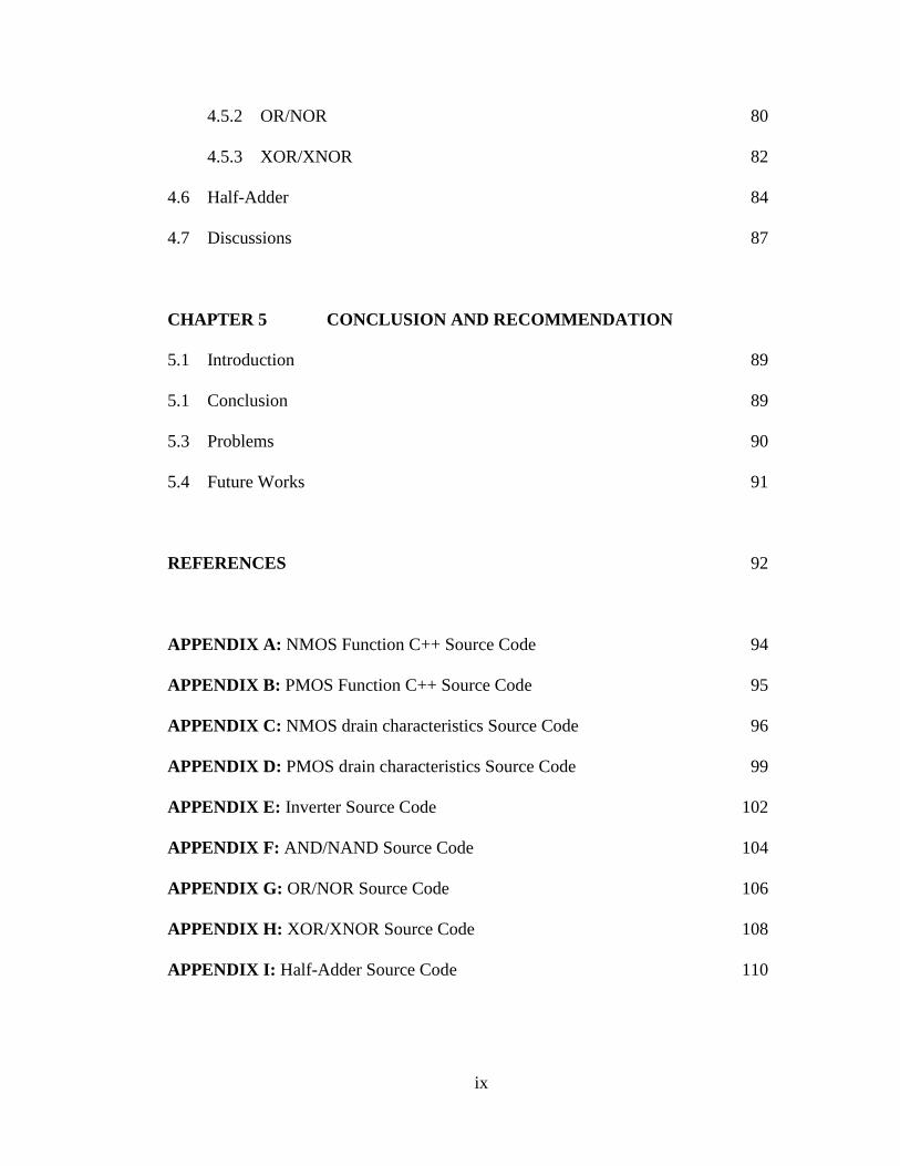
ix
4.5.2 OR/NOR 80
4.5.3 XOR/XNOR 82
4.6 Half-Adder 84
4.7 Discussions 87
CHAPTER 5 CONCLUSION AND RECOMMENDATION
5.1 Introduction 89
5.1 Conclusion 89
5.3 Problems 90
5.4 Future Works 91
REFERENCES 92
APPENDIX A: NMOS Function C++ Source Code 94
APPENDIX B: PMOS Function C++ Source Code 95
APPENDIX C: NMOS drain characteristics Source Code 96
APPENDIX D: PMOS drain characteristics Source Code 99
APPENDIX E: Inverter Source Code 102
APPENDIX F: AND/NAND Source Code 104
APPENDIX G: OR/NOR Source Code 106
APPENDIX H: XOR/XNOR Source Code 108
APPENDIX I: Half-Adder Source Code 110
x
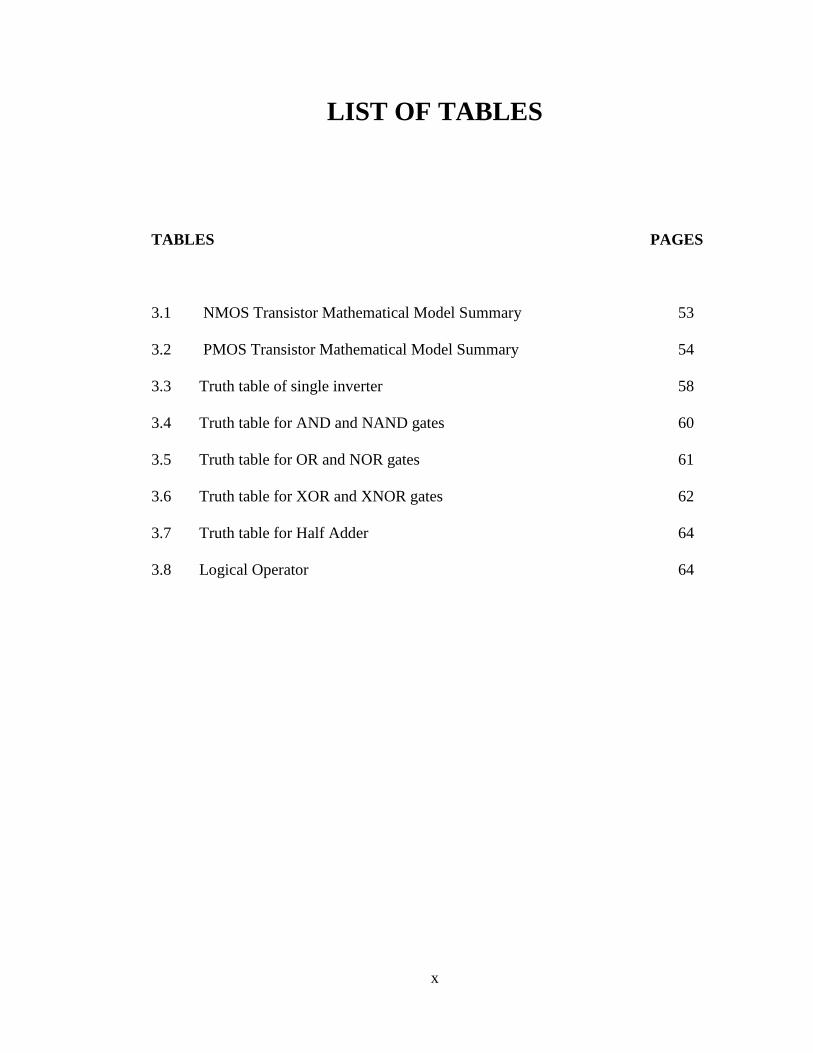
LIST OF TABLES
TABLES PAGES
3.1 NMOS Transistor Mathematical Model Summary 53
3.2 PMOS Transistor Mathematical Model Summary 54
3.3 Truth table of single inverter 58
3.4 Truth table for AND and NAND gates 60
3.5 Truth table for OR and NOR gates 61
3.6 Truth table for XOR and XNOR gates 62
3.7 Truth table for Half Adder 64
3.8 Logical Operator 64
xi
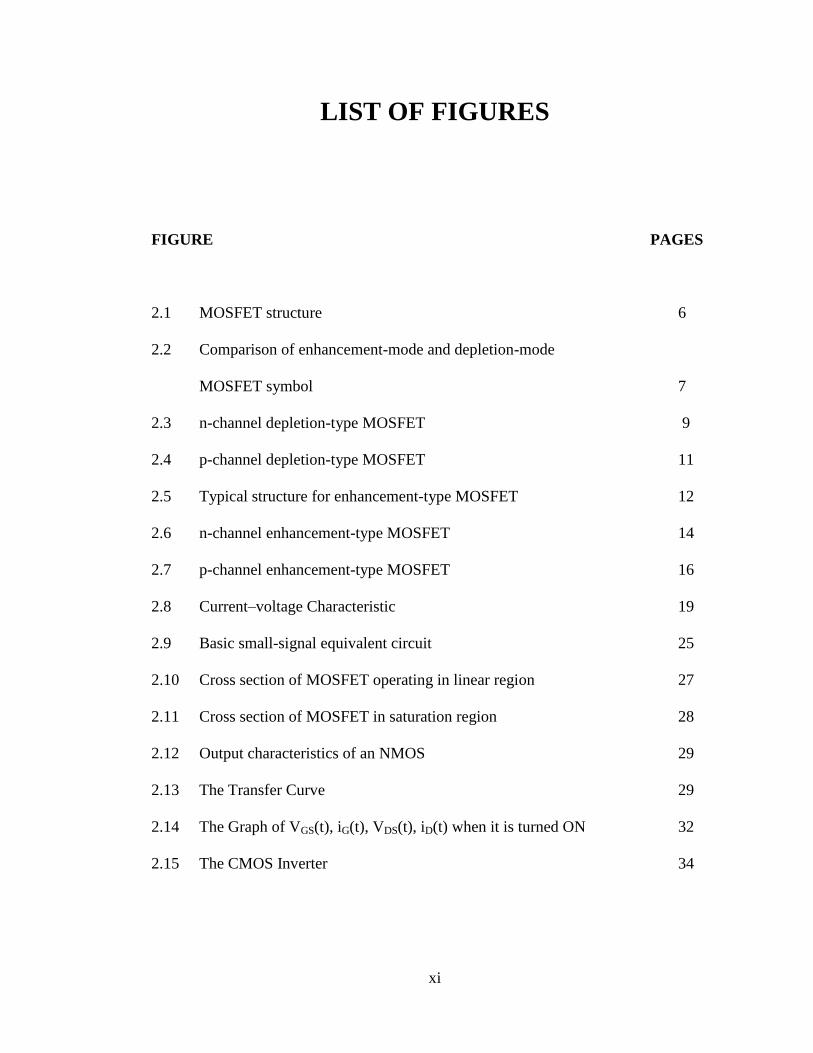
LIST OF FIGURES
FIGURE PAGES
2.1 MOSFET structure 6
2.2 Comparison of enhancement-mode and depletion-mode
MOSFET symbol 7
2.3 n-channel depletion-type MOSFET 9
2.4 p-channel depletion-type MOSFET 11
2.5 Typical structure for enhancement-type MOSFET 12
2.6 n-channel enhancement-type MOSFET 14
2.7 p-channel enhancement-type MOSFET 16
2.8 Current–voltage Characteristic 19
2.9 Basic small-signal equivalent circuit 25
2.10 Cross section of MOSFET operating in linear region 27
2.11 Cross section of MOSFET in saturation region 28
2.12 Output characteristics of an NMOS 29
2.13 The Transfer Curve 29
2.14 The Graph of VGS(t), iG(t), VDS(t), iD(t) when it is turned ON 32
2.15 The CMOS Inverter 34
xii
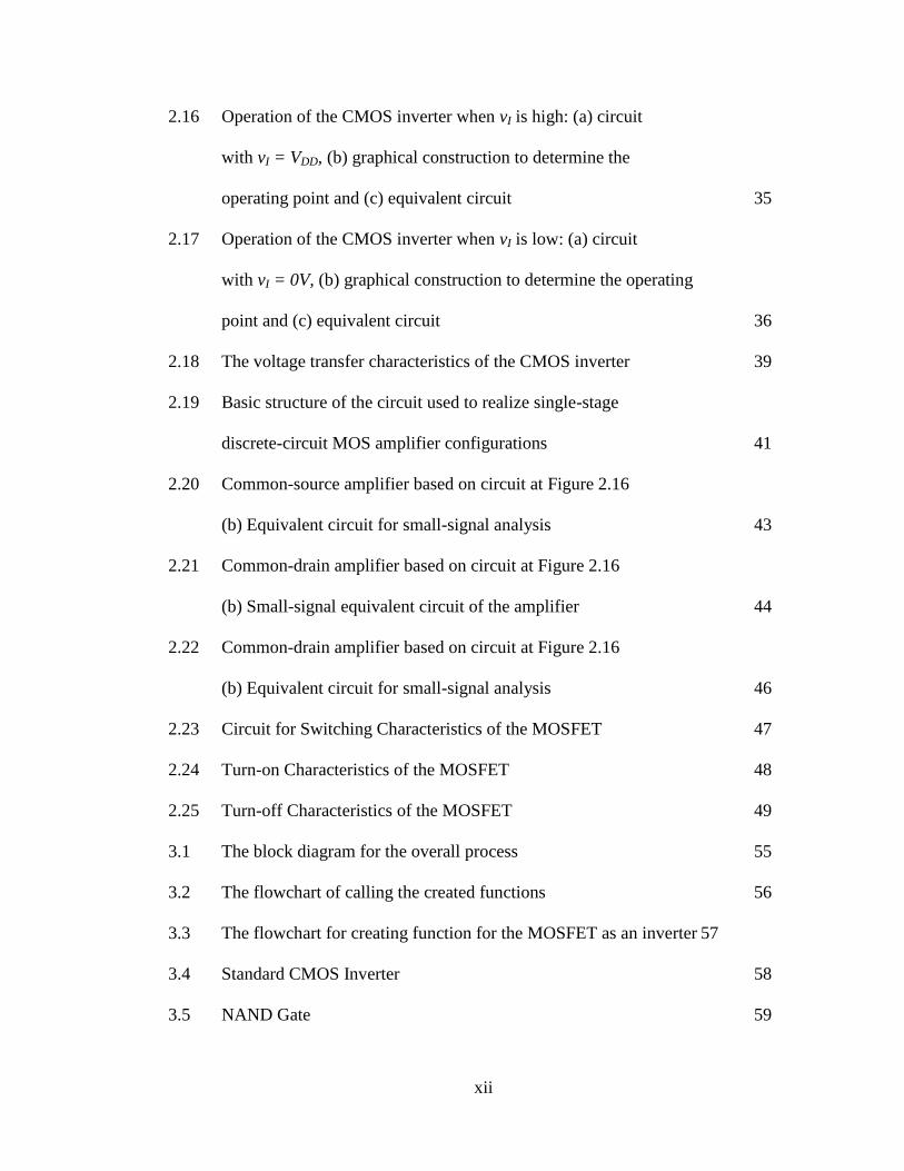
2.16 Operation of the CMOS inverter when vI is high: (a) circuit
with vI = VDD, (b) graphical construction to determine the
operating point and (c) equivalent circuit 35
2.17 Operation of the CMOS inverter when vI is low: (a) circuit
with vI = 0V, (b) graphical construction to determine the operating
point and (c) equivalent circuit 36
2.18 The voltage transfer characteristics of the CMOS inverter 39
2.19 Basic structure of the circuit used to realize single-stage
discrete-circuit MOS amplifier configurations 41
2.20 Common-source amplifier based on circuit at Figure 2.16
(b) Equivalent circuit for small-signal analysis 43
2.21 Common-drain amplifier based on circuit at Figure 2.16
(b) Small-signal equivalent circuit of the amplifier 44
2.22 Common-drain amplifier based on circuit at Figure 2.16
(b) Equivalent circuit for small-signal analysis 46
2.23 Circuit for Switching Characteristics of the MOSFET 47
2.24 Turn-on Characteristics of the MOSFET 48
2.25 Turn-off Characteristics of the MOSFET 49
3.1 The block diagram for the overall process 55
3.2 The flowchart of calling the created functions 56
3.3 The flowchart for creating function for the MOSFET as an inverter 57
3.4 Standard CMOS Inverter 58
3.5 NAND Gate 59
xiii
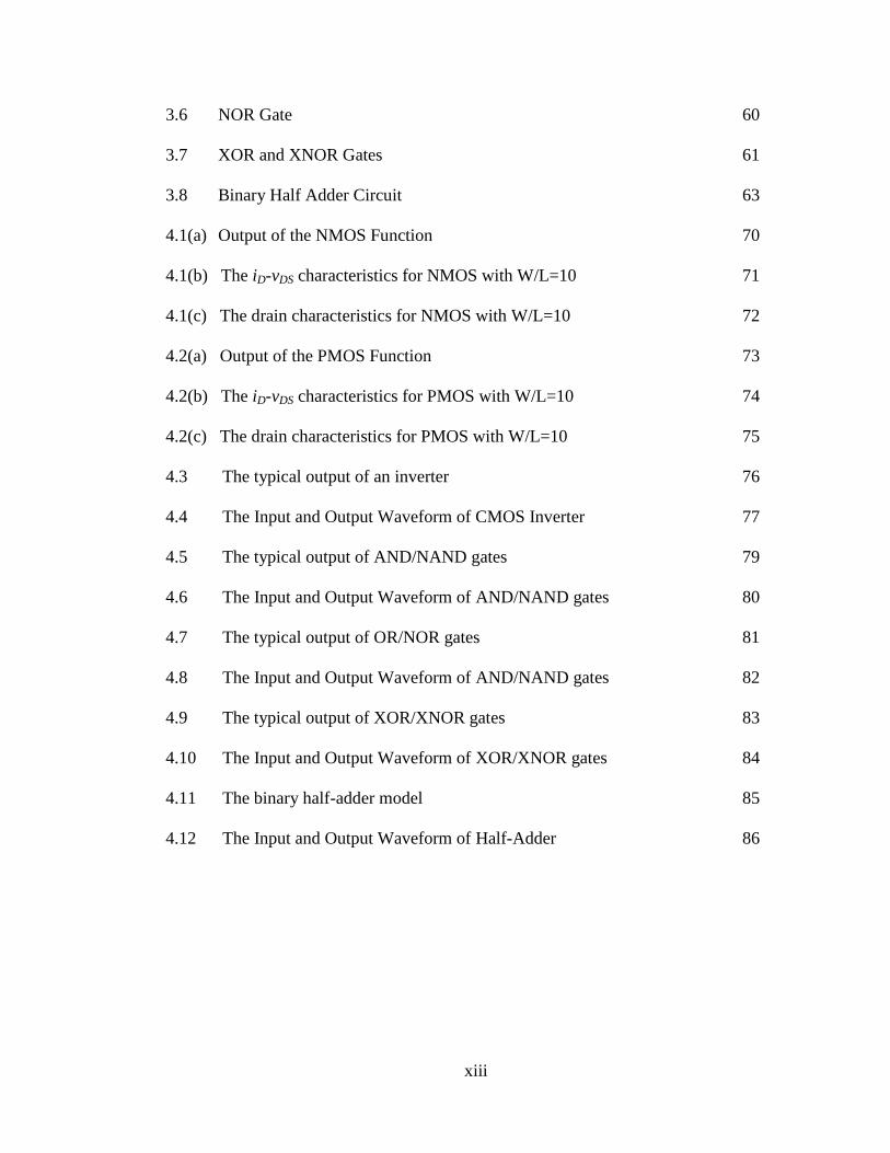
3.6 NOR Gate 60
3.7 XOR and XNOR Gates 61
3.8 Binary Half Adder Circuit 63
4.1(a) Output of the NMOS Function 70
4.1(b) The iD-vDS characteristics for NMOS with W/L=10 71
4.1(c) The drain characteristics for NMOS with W/L=10 72
4.2(a) Output of the PMOS Function 73
4.2(b) The iD-vDS characteristics for PMOS with W/L=10 74
4.2(c) The drain characteristics for PMOS with W/L=10 75
4.3 The typical output of an inverter 76
4.4 The Input and Output Waveform of CMOS Inverter 77
4.5 The typical output of AND/NAND gates 79
4.6 The Input and Output Waveform of AND/NAND gates 80
4.7 The typical output of OR/NOR gates 81
4.8 The Input and Output Waveform of AND/NAND gates 82
4.9 The typical output of XOR/XNOR gates 83
4.10 The Input and Output Waveform of XOR/XNOR gates 84
4.11 The binary half-adder model 85
4.12 The Input and Output Waveform of Half-Adder 86
1
CHAPTER 1
INTRODUCTION
1.1 Background
Digital circuits are comprised of millions of transistors. Transistors are made of
MOSFETs (Metal Oxide Semiconductor Field-Effect Transistors). This is a particular
kind of FETs (Field-Effect Transistors) that controls the current between two points.
The FET operates by the effects of an electric field on the flow of electrons through a
single type of semiconductor material. This is why the FET is sometimes called a
unipolar transistor. MOSFET is extremely popular in the industry. It uses the integrated-
circuit technology called microelectronic that capable of producing circuits that contain
millions of components in a small piece of silicon (known as a silicon chip) whose area
is on the order of 100mm2 [11].
MOSFETs are either NMOS (n-channel) or PMOS (p-channel) transistors,
which are fabricated as individually packaged discrete components for high power
2
applications as well as by the hundreds of millions inside a single chip. Compared to
BJTs (Bipolar Junction Transistor) or other devices, MOSFETs are small can be well
packed together on the high density chip thus the MOSFET manufacturing process is
relatively simple.
1.2 History of MOSFETs
A conceptually similar structure was first proposed and patented by Lilienfeld
[4] and Heil [2] in 1930, but was successfully demonstrated until 1960 where the first
MOSFET was fabricated by Kahng at Bell Laboratory [3]. The main technological
problem was the control and reduction of the surface states at the interface between the
oxide and the semiconductor.
For the last four decades, the MOSFET circuit technology has dramatically
changed. The MOSFETs has evolved from the PMOS in the 1960’s to the NMOS in the
1070’s. Another important development in the evolution of the MOSFETs is the
replacement of metal gate with poly-silicon gate. Early MOSFETs used aluminum as a
gate electrode, hence the name MOSFET. However the use of heavily doped poly-
silicon as a gate material opened a whole new vista and allowed tremendous
improvement in scalability of MOSFETs and technology.
Starting with ten-micron PMOS process with an aluminum gate and a single
metallization layer around 1970, the technology has evolved into tenth-micron self-
3
aligned-gate complementary-MOS (CMOS) process with up to five metallization levels.
The transistor from dopant diffusion to ion implantation, from thermal oxidation to
oxide deposition, from metal gate to a poly-silicon gate, from wet chemical etching to
dry etching and more recently from aluminum (with 2% copper) wiring to copper has
provided vastly superior analog and digital CMOS circuits. CMOS forms the basis of
the vast majority of all high density ICs manufactured today [12].
1.3 Objectives
The main objectives of this project are:
i) To model the MOSFETs characteristics by using C++
ii) To model the operating functions of MOSFETs with C++ and implement
for inverter application.
1.4 Organization of The Report
This document is organized in such a way to represent the development stages of
the whole project. The report can be categorized into two stages; theory and
implementation. The first stage consists of Chapter 1, 2 and 3 whereas the second stage
covers Chapter 4 and 5.
4
In Chapter 1, a brief background of MOSFETs is introduced by giving a general
overview of MOSFETs evolution via the microelectronic technology. Next, Chapter 2
discusses the theory of MOSFET in term of its characteristics and applications. This
chapter gives a better view understanding the operation of MOSFET and how these
characteristics give privileges to MOSFET to be implemented as switches, amplifiers
and logic inverter.
For the implementation part, Chapter 3 focuses more on the methodology of
modeling the MOSFETs using Microsoft Visual C++ software. This chapter also
represents a step-by-step approach applied to use the user-defined functions for
MOSFETs analysis. The functions created afterward will be tested by putting in values
and the outputs are then analyzed in the Chapter 4. Discussions on problems,
modifications and improvement on the source codes are generally explained. Finally,
last but not least, Chapter 5 concludes the execution of the project. It also gives some
recommendations on improvements and future works that can be made to the project in
the future.
5
CHAPTER 2
LITERATURE REVIEW
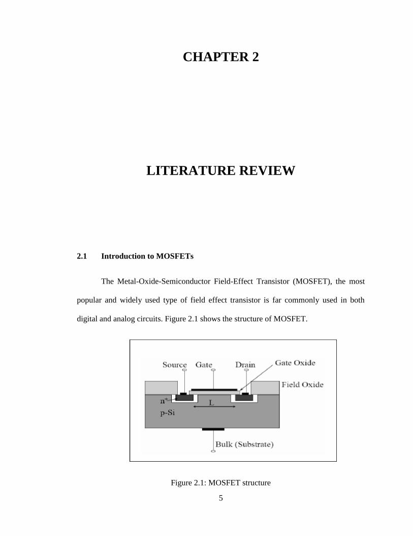
2.1 Introduction to MOSFETs
The Metal-Oxide-Semiconductor Field-Effect Transistor (MOSFET), the most
popular and widely used type of field effect transistor is far commonly used in both
digital and analog circuits. Figure 2.1 shows the structure of MOSFET.
Figure 2.1: MOSFET structure
6
The MOSFET is composed of a channel of n-type or p-type semiconductor
material, fabricated as individually packaged discrete components for high power
applications as well as by the hundreds of millions inside a single chip (IC), and is
accordingly called an NMOS or a PMOS. Usually the semiconductor of choice is
silicon, but some chip manufactures, most notably IBM, have begun to use a mixture of
silicon and germanium (SiGe) in MOSFET channels. Unfortunately, many
semiconductors with better electrical properties than silicon, such as gallium arsenide,
do not form good gate oxides and thus are not suitable for MOSFETs.
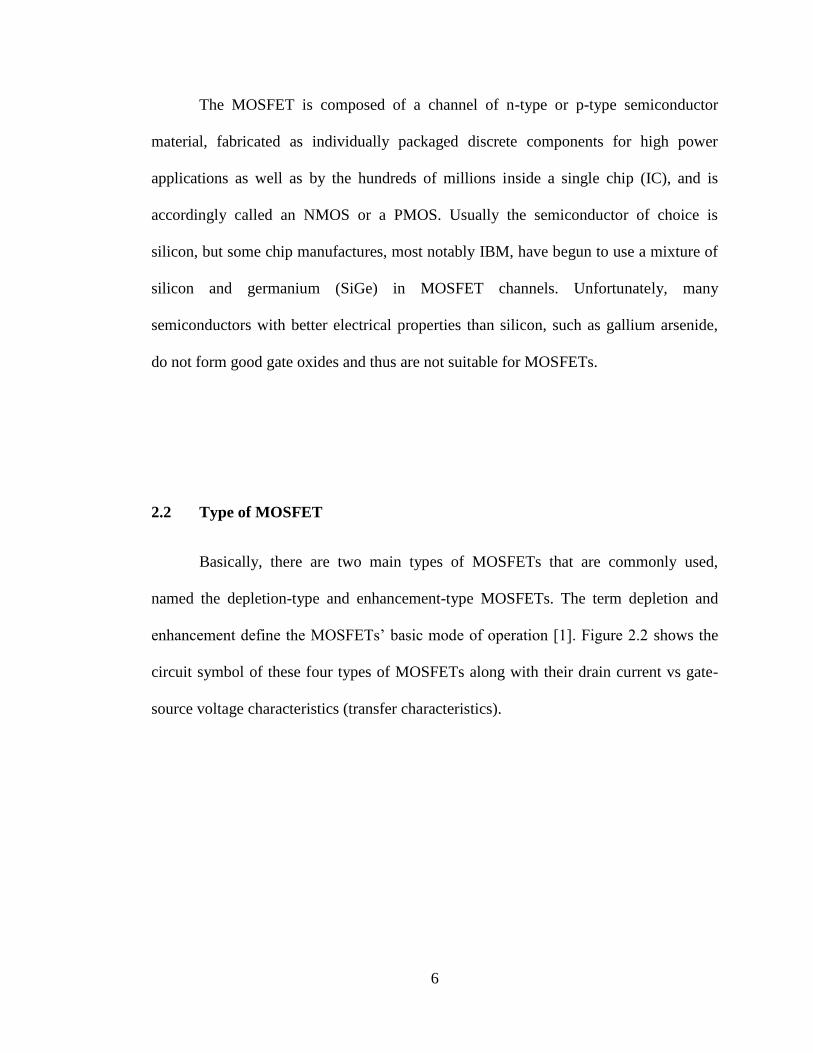
2.2 Type of MOSFET
Basically, there are two main types of MOSFETs that are commonly used,
named the depletion-type and enhancement-type MOSFETs. The term depletion and
enhancement define the MOSFETs’ basic mode of operation [1]. Figure 2.2 shows the
circuit symbol of these four types of MOSFETs along with their drain current vs gate-
source voltage characteristics (transfer characteristics).
7
Figure 2.2: Comparison of enhancement-mode and depletion-mode MOSFET symbol
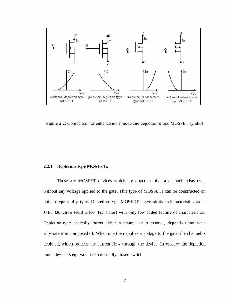
2.2.1 Depletion-type MOSFETs
These are MOSFET devices which are doped so that a channel exists even
without any voltage applied to the gate. This type of MOSFETs can be constructed on
both n-type and p-type. Depletion-type MOSFETs have similar characteristics as in
JFET (Junction Field Effect Transistor) with only few added feature of characteristics.
Depletion-type basically forms either n-channel or p-channel, depends upon what
substrate it is composed of. When one then applies a voltage to the gate, the channel is
depleted, which reduces the current flow through the device. In essence the depletion
mode device is equivalent to a normally closed switch.
8
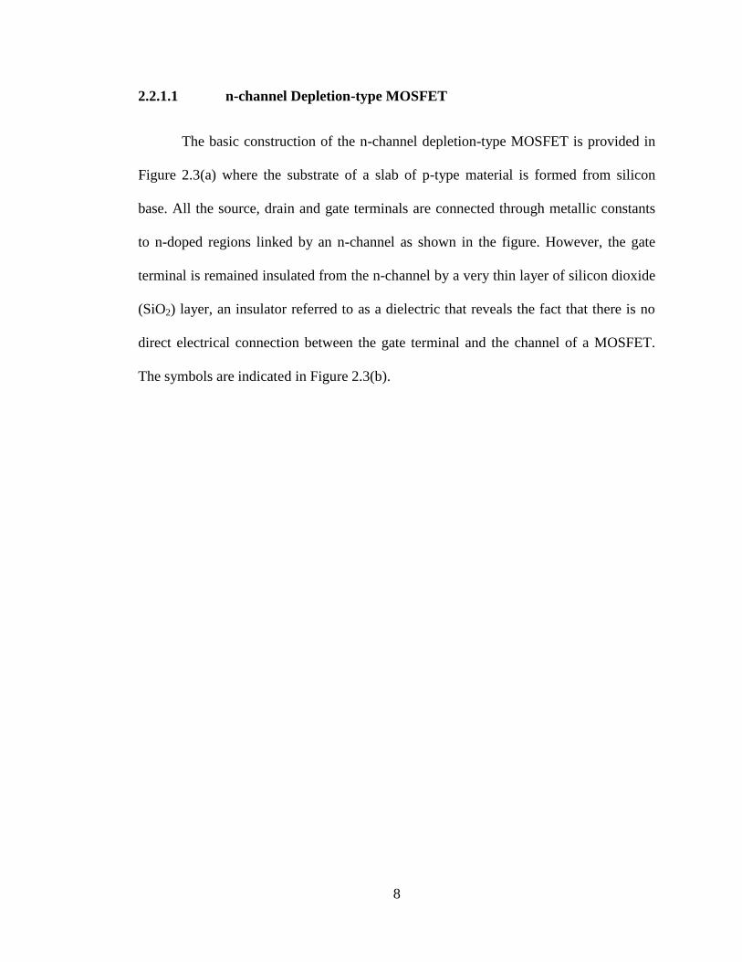
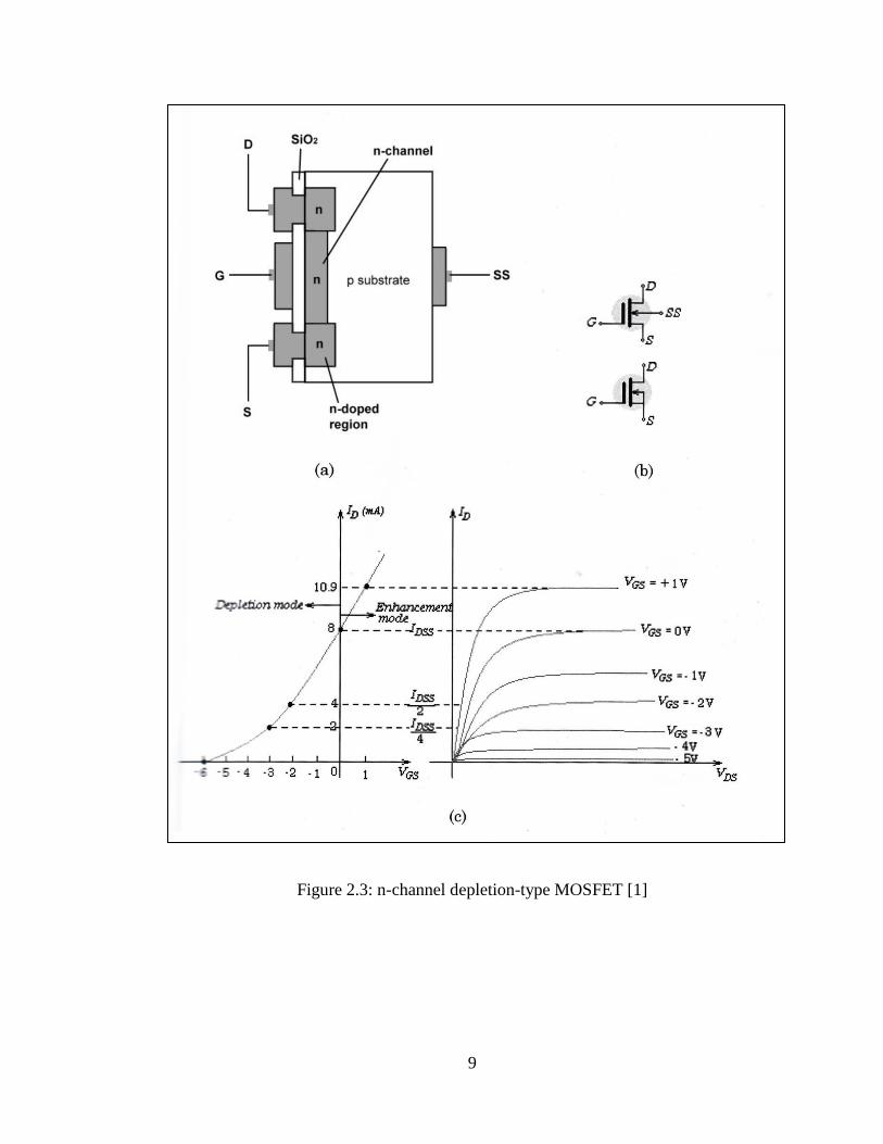
2.2.1.1 n-channel Depletion-type MOSFET
The basic construction of the n-channel depletion-type MOSFET is provided in
Figure 2.3(a) where the substrate of a slab of p-type material is formed from silicon
base. All the source, drain and gate terminals are connected through metallic constants
to n-doped regions linked by an n-channel as shown in the figure. However, the gate
terminal is remained insulated from the n-channel by a very thin layer of silicon dioxide
(SiO2) layer, an insulator referred to as a dielectric that reveals the fact that there is no
direct electrical connection between the gate terminal and the channel of a MOSFET.
The symbols are indicated in Figure 2.3(b).
9
Figure 2.3: n-channel depletion-type MOSFET [1]