kolej universiti teknologi tun hussein...
TRANSCRIPT

KOLEJ UNIVERSITI TEKNOLOGI TUN HUSSEIN ONN
JUDUL:
Saya
BORANG PENGESAHAN STATUS TESIS·
SIMULATION STUDIES OF 30 MHz PHASE-LOCKED LOOP COHERENT RECEIVER.
SESI PENGAJIAN: __ 2_0_04_/2_0_0_5_
F AUZI BIN ABDUL W ARAB (HURUF BESAR)
mengaku membenarkan tesis (S~u3;alOl.;a Hmla/Smjana molrter Falsaf?h)* ini disimpan di Perpustakaan dengan syarat-syarat kegunaan seperti berikut:
1. Tesis adalah hakrnilik Kolej Universiti Teknologi Tun Hussein Onn. 2. Perpustakaan dibenarkan membuat salinan untuk tujuan pengajian sahaja. 3. Perpustakaan dibenarkan membuat salinan tesis ini sebagai bahan pertukaran antara
institusi pengajian tinggi. 4. **Sila tandakan (v"')
D SULIT
D TERHAD
(Mengandungi maklumat yang berdarjah keselamatan atau kepentingan Malaysia seperti yang terrnaktub di dalam ART A RAHSIA RASMI 1972)
(Mengandungi maklumat TERHAD yang telah ditentukan oleh organisasilbadan di mana penyelidikan dijalankan)
II ./ II TIDAK TERHAD
jJkA2. (T ANDAT ANGAN PENULIS)
Alamat Tetap: 41 P ARIT PUNGGUR, JALAN ABDUL RAHMAN, 84150 MUAR, JOHOR.
Tarikh: 4 APRIL 2005
CATATAN:
~ (TANDATANGAN PENYELlA)
PM. DR. ZAINAL ALAM HARON
Nama Penyelia
Tarikh: 4 APRIL 2005
* **
Potong yang tidak berkenaan. Jika tesis ini SULIT atau TERHAD, sila lampirkan surat daripada pihak berkuasa/organisasi berkenaan dengan menyatakan sekali tempoh tesis ini perlu dikelaskan sebagai at au TERHAD.
• Tesis dirnaksudkan sebagai tesis bagi Ijazah doktor Falsafah dan Sarjana secara Penyelidikan, atau disertasi bagi pengajian secara kerja kursus dan penyelidikan, atau Laporan Projek SaIjana Muda (PSM).
" I hereby declare that I have read this thesis and acknowledged it has achievcd the
scope and quality for the award of the Degree of Master of Electrical Engineering."
Signature
Supervisor
Date
-'
PM. DR. ZAINAL ALAM HARON
APRIL 2005
SIMULATION STUDIES OF 30 JY1Hz PHASE-LOCKED LOOP COHERENT
RECEIVER
F AUZI BIN ABDUL W ARAB
This proj ect report is submitted in partial fulfilment of the requirements for the
award of Master of Electrical Engineering
Fakulti Kejuruteraan Elektrik dan Elektronik
Kolej Universiti Teknologi Tun Hussein Onn
APRIL, 2005

"I hereby declare that this project is my original work except for the notations and
summaries which I have stated the sources" .
Signature
Name
Date
....... ~ .. : ........... . Fauzi bin Abdul Wahab
4th April 2005
11

111
ACKNOWLEDGEMENT
First of all ALHAMDULILLAH my prayers to ALLAH for the
opportunities. I would like to thank my parents for bringing me to this world and for
being there whenever I needed most. Especially for the advices about life. To my
wife, Zarita binti Mohd Kosnll, my two children, Hakim Syahmi and Hanis
Syadiyah for the patience, inspiration and moral support. And not forgetting my
brothers and sisters. My Supervisor, P.M. Dr Zainal Alam bin Haron for the wise
ideas and knowledge. To all my lecurers, you are like my elder brothers and sisters
and I thank you all for the knowledge and experience shared. And last but not least,
to my friends, thank you for your prayers.

IV
ABSTRACT
Phase-Locked Loop or in short PLL is a vital part in electronics system
mainly in communication system in getting back the transmitted signal. As a whole,
it is basically a closed loop frequency control system where its function is based on
the phase sensitive detection of phase difference between the input signal
(transmitted signal) and the output of the controlled oscillation. Although the system
had been around since 1930's, implemented by the French Engineer, H. De
Bellescise, but still, until today further development is in progress in achieving better
response and performance in retrieving and synchronising transmitted signals. The
purpose of this project is to familiarise in designing and constructing a 30 MHz
Phase-Locked Loop Coherent Receiver by computer simulation, taking account the
requirements for each building block of a PLL system, the stability of the system and
the response of the system. To achieve this, the process includes simple and direct
calculations, and circuit simulations observation. Results are represented in graphs
and are analysed.
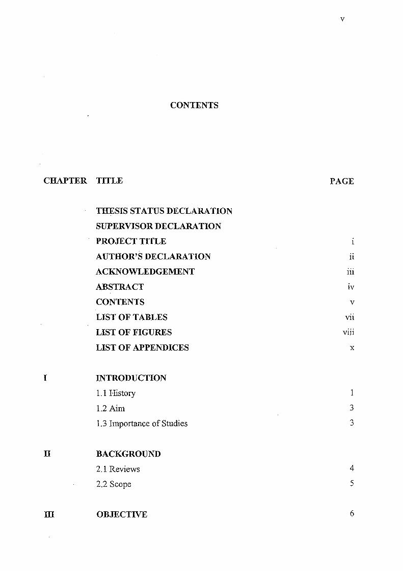
CONTENTS
CHAPTER TITLE
I
n
ill
THESIS STATUS DECLARATION
SUPERVISOR DECLARATION
PROJECT TITLE
AUTHOR'S DECLARATION
ACKNOWLEDGEMENT
ABSTRACT
CONTENTS
LIST OF TABLES
LIST OF FIGURES
LIST OF APPENDICES
INTRODUCTION
1.1 History
1.2 Aim
1.3 hnportance of Studies
BACKGROUND
2.1 Reviews
2.2 Scope
OBJECTIVE
v
PAGE
1
11
111
lV
v
Vll
Vl11
x
1
3
3
4
5
6

IV
V
VI
METHODOLOGY
4.1 The Architecture Design
4.2 The Phase Detector
4.3 The Low-Pass Filter
4.4 The Voltage Controlled Oscillator
RESULTS AND DISCUSSION
5.1 The Low-Pass Filter
5.2 Oscillation Detennination
5.3 Amplifier Circuit Design
5.4 Voltage Controlled Oscillator Components
Determination
5.5 Results
5.6 Discussions
CONCLUSION
REFERENCE
APPENDICES
VI
8
8
10
10
13
14
15
20
24
53
55
57
58
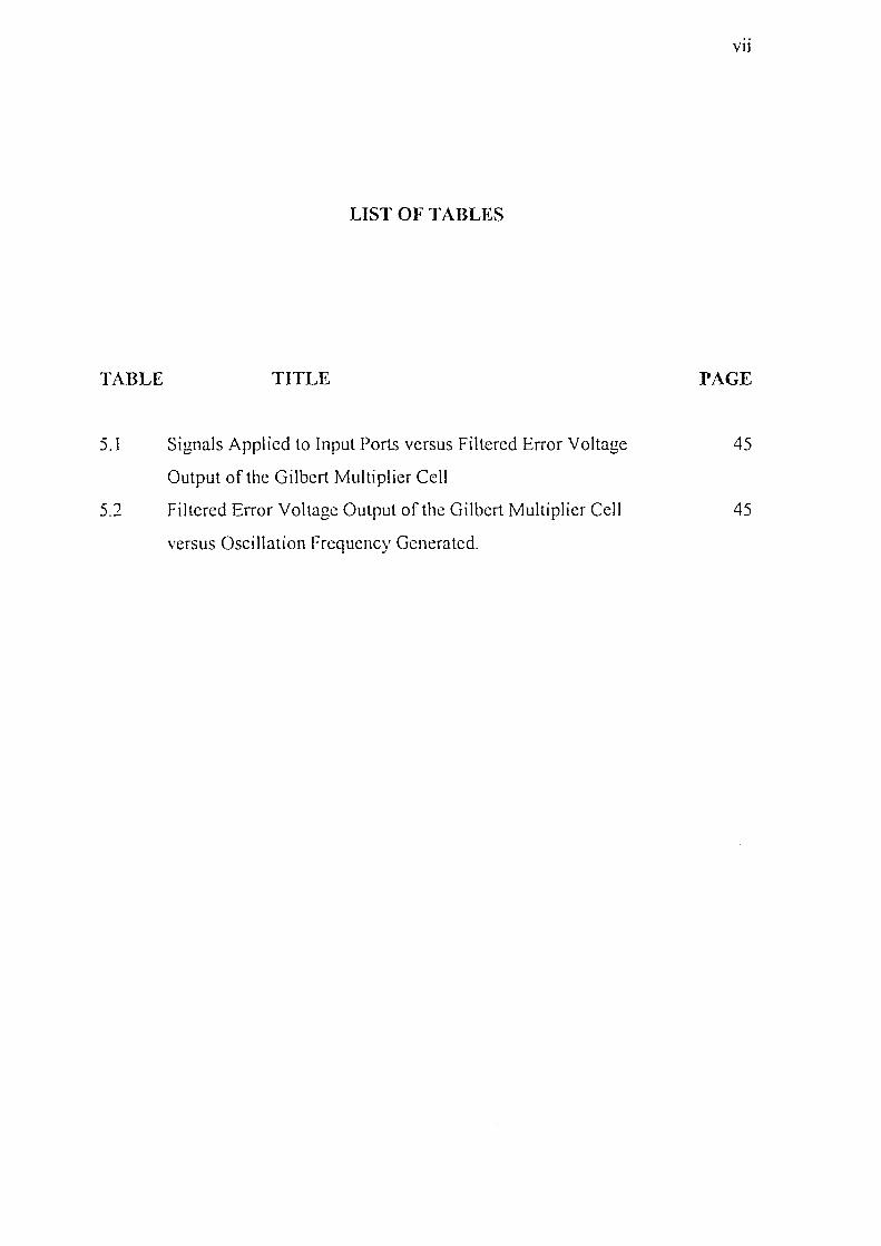
LIST O:F TABLES
TABLE TITLE
5.1 Signals Applied to Input Ports versus Filtered Error Voltage
Output of the Gilbert Multiplier Cell
5.2 Filtered Error Voltage Output of the Gilbert Multiplier Cell
versus Oscillation Frequency Generated.
VB
PAGE
45
45
Vlll
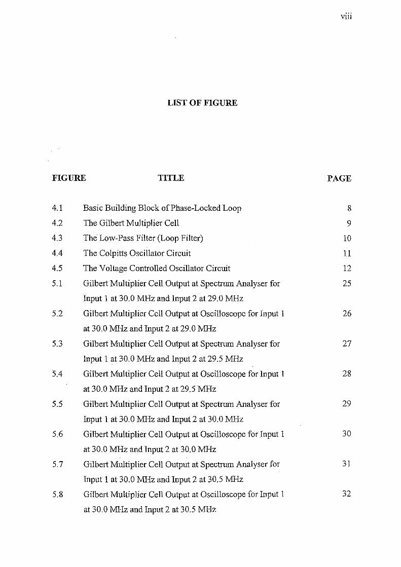
LIST OF FIGURE
FIGURE TITLE PAGE
4.1 Basic Building Block of Phase-Locked Loop 8
4.2 The Gilbert Multiplier Cell 9
4.3 The Low-Pass Filter (Loop Filter) 10
4.4 The Colpitts Oscillator Circuit 11
4.5 The Voltage Controlled Oscillator Circuit 12
5.1 Gilbert Multiplier Cell Output at Spectrum Analyser for 25
Input 1 at 30.0 MHz and Input 2 at 29.0 MHz
5.2 Gilbert Multiplier Cell Output at Oscilloscope for Input 1 26
at 30.0 MHz and Input 2 at 29.0 1v1Hz
5.3 Gilbert Multiplier Cell Output at Spectrum Analyser for 27
Input 1 at 30.0 MHz and Input 2 at 29.5 MHz
5.4 Gilbert Multiplier Cell Output at Oscilloscope for Input 1 28
at 30.0 MHz and Input 2 at 29.51v1Hz
5.5 Gilbert Multiplier Cell Output at Spectrum Analyser for 29
Input 1 at 30.0 MHz and Input 2 at 30.0 MHz
5.6 Gilbert Multiplier Cell Output at Oscilloscope for Input 1 30
at 30.0 MHz and Input 2 at 30.0 MHz
5.7 Gilbert Multiplier Cell Output at Spectrum Analyser for 31
Input 1 at 30.0 MHz and Input 2 at 30.5 MHz
5.8 Gilbert Multiplier Cell Output at Oscilloscope for Input 1 32
at 30.0 MHz and Input 2 at 30.5 MHz
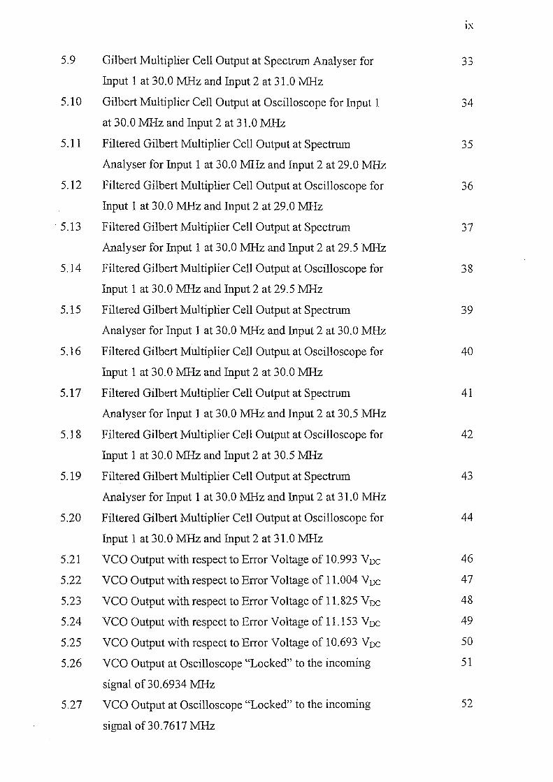
lX
5.9 Gilbert Multiplier Cell Output at Spectrum Analyser for ...,.., .).)
Input 1 at 30.0 MHz and Input 2 at 31.0 MHz
5.10 Gilbert Multiplier Cell Output at Oscilloscope for Input 1 34
at 30.0:MHz and Input 2 at 31.0 MHz
5.11 Filtered Gilbert Multiplier Cell Output at Spectrum 35
Analyser for Input 1 at 30.0 WIz and Input 2 at 29.0 MHz
5.12 Filtered Gilbert Multiplier Cell Output at Oscilloscope for 36
Input 1 at 30.0 MHz and Input 2 at 29.0 MHz
5.13 Filtered Gilbert Multiplier Cell Output at Spectrum 37
Analyser for Input 1 at 30.0 MHz and Input 2 at 29.5 MHz
5.14 Filtered Gilbert Multiplier Cell Output at Oscilloscope for 38
Input 1 at 30.0 MHz and Input 2 at 29.5:MHz
5.15 Filtered Gilbert Multiplier Cell Output at Spectmm 39
Analyser for Input 1 at 30.0 MHz and Input 2 at 30.0 MHz
5.16 Filtered Gilbert Multiplier Cell Output at Oscilloscope for 40
Input 1 at 30.0 MHz and Input 2 at 30.0 MHz
5.17 Filtered Gilbert Multiplier Cell Output at Spectmm 41
Analyser for Input 1 at 30.0 MHz and Input 2 at 30.5 MHz
5.18 Filtered Gilbert Multiplier Cell Output at Oscilloscope for 42
Input 1 at 30.0 MHz and Input 2 at 30.5 MHz
5.19 Filtered G.ilbert Multiplier Cell Output at Spectrum 43
Analyser for Input 1 at 30.0 MHz and Input 2 at 31.0 MHz
5.20 Filtered Gilbert Multiplier Cell Output at Oscilloscope for 44
Input 1 at 30.0 MHz and Input 2 at 31.0 MHz
5.21 VCO Output with respect to Error Voltage of 10.993 VDC 46
5.22 VCO Output with respect to Error Voltage of 11.004 Voc 47
5.23 VCO Output with respect to Error Voltage of 11.825 Voc 48
5.24 VCO Output with respect to Error Voltage of 11.153 Voc 49
5.25 VCO Output with respect to Error Voltage of 10.693 Voc 50
5.26 VCO Output at Oscilloscope "Locked" to the incoming 51
signal of30.6934 MHz
5.27 VCO Output at Oscilloscope "Locked" to the incoming 52
signal of 30.7617 MHz
x
LIST OF APPENDICES
APPENDIX TITLE PAGE
A 2N2222, 2N2222A NPN Switching Transistor Data Sheet 59
B Silicon 25V Hyperabrupt Varactor Diodes (830 Series) Data 67
Sheet
C 1N4001GP-1N4007GP Diode Data Sheet 73
D Introduction to The MultiSllv1® Interface 79
E MultiSIM® Spectrum Analyser 81
F MultiSllv1® Oscilloscope 87
CHAPTER I
INTRODUCTION
1.1 IIistOl:Y
Phase-Locked Loop has been implemented by a French Engineer in 1932.
This system replaced several other receiver system inventions, namely the super
heterodyne radio receiver and later the homo dyne or synchrodyne receivers. The
"old" radio receivers first invented in 1918 by E. H. Armstrong while serving the
Army Signal Corps in France. These classic designs consist of local oscillator, a
mixer and audio amplifier. Their basic concept of operation was when the input
signal and local oscillator were mixed at the same phase and frequency, the output
was an exact audio representation of the modulated carrier.
It was considered a perfect system initially, but then the synchronous
reception became difficult due to tiny drift in frequency of the local oscillator after a
period of time in operation. Phase-Locked Loop is an evolution to solving oscillator
problems. The key to the successful system is providing correction voltage feedback
(or also known as Error Voltage signal) to the oscillator from the phase detector and
thus keeping it on the right frequency. Although the homo dyne or synchrodyne
receivers seemed superior to the super heterodyne receivers, the cost of constructing

Phase-Locked Loop circuit outweighed its advantages that made the Phase
Locked Loop became more popular among designers and manufacturers.
2
In 1940's, the first commonly usage of Phase-Locked Loop was in the
synchronisation of the horizontal and vertical sweep oscillators for television system.
Since then, the electronic phase-locked loop principle has been extended to other
,applications. AM and FM Demodulators, FSK Decoder, Touch-Tone® Decoder,
, motor speed controller, Robotics and Radio Control transmitter and receivers. In the
wireless world, Phase-Locked Loop is used for
1. Carrier Synchronisation
2. Carrier Recovery
3. Frequency division and multiplication
4. Demodulation
The first Phase-Locked Loops were analogue but since 1970' s, integrated circuits
have been available to perform the same functions on a chip. These are called digital
PLLs. There are 4 different types ofPLLs.
1. The Linear or Analogue PLL (LPLL)
2. The Digital PLL (DPLL)
3. The All-Digital PLL (ADPLL)
4. Software PLL (SPLL)
The concept basis behind each of the first three is the same. They are specified
by the same standard parameters such as loop bandwidth and damping factor. But
Software PLL is usually implemented by a microcontroller, microcomputer or digital
signal processor (DSP), it is generally considered to be an all-digital and it can
perform like a LPLL, a DPLL or and ADPLL. Therefore SPLL is the most universal
type ofPLL but the limitation is, it needs computer algorithm perfonning the PLL
function to be executed at least once in every period of the input signal of the PLL
1.2 Aim
The purpose of this project is to familiarise with designing of a Phase
Locked-Loop system and as a guide, the focus is on a 30MHz coherent receiver.
1.3 Importance of Studies
3
The project benefits is to adopting and gaining the experience of designing a
Phase-Locked Loop system by the practical approach and employ some fundamental
knowledge and theories. And also engineer them in building the basic blocks of a
Phase Locked-Loop system.
4
CHAPTERll
BACKGROUND
2.1 Revievvs
Since the system had been invented over the past 70 years, a lot of articles
and books had been written by numerous authors. Among them, Garth Nash, an
Application Engineer in his "Phase-Locked Loop Design Fundamental", Application
Note, Motorola Inc 1994. He concluded and described the basic control techniques
required for Phase-Locked Loop design. He also presented the criteria for selection
of the optimum type of loop and methods for establishing the desired perfonnance
characteristics.
Books written by R. E. Best in "Phase-Locked Loop, Design, Simulation and
Applications", 3rd edition, McGraw Hill,1997 and "Phaselock Technique", by F. M.
Gardner, 2nd edition, 1979, John Wiley & Sons, New York provides crucial and
important theories in designing the Phase-Locked Loop system although they were
deeply describing the operation of a Phase Locked-Loop system.

5
And, Mark Curtin and PaulO' Brien in their "Phase-Locked Loops for High
Frequency Receivers and Transmitters Part 1,2 & 3" Analog Dialog 1999,
emphasised the phase noise, reference spurs and output leakage current. Perhaps this
can be adopted to the 30 J\1hz Phase-Locked Loop system design as their conclusion
were based on high frequencies system.
2.2 Scope
The scope of this project is to study and design a 30 MHz Phase-Locked
Loop coherent receiver by computer simulation, looking into requirements, response
and behaviour for each individual building block of the Phase-Locked Loop.
CHAPTERll
OBJECTIVE
To support the aim of this project, these are the objectives identified.
1. To study the behaviour of the individual building block of the Phase-Locked
Loop system i.e. The Phase Detector, the Loop Filter and the Voltage
Controlled Oscillator.
2. To calculate the circuit requirements using the right formulas to achieve the
response of each building block circuit for the 30 1v1Hz Phase-Locked Loop
coherent receiver.
3. Simulate each circuit design of the building block of the Phase-Locked Loop
and their combinations. At this stage, make changes or modification if
necessary to the design.
6
7
CHAPTER IV
METHODOLOGY
The designing uses direct approach in assembling them. By looking into the
response of each basic building block, and the observations pursued onto the overall
system response. In the first stage, simple calculations were made for the required
components values. Secondly, constructing the circuit for each building block of the
Phase-Locked Loop for computer simulations and analysing the behaviour and
response of each building block of the Phase-Locked Loop.
Having the advantages and capability to add non-existence components to its
library, MultiSIM ™ & Electronics Workbench ™ (MultiSIM 2001 Education
Version) had been chosen. The components' parameters and Spice Models can be
easily obtained from the respective manufacturers.
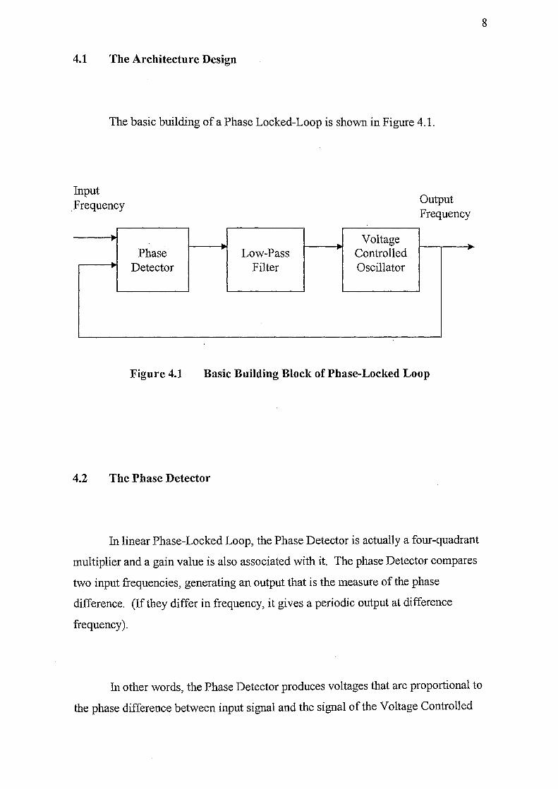
4.1 The Architecture Design
The basic building of a Phase Locked-Loop is shown in Figure 4.1.
Input ,Frequency
.. Phase
Detector Low-Pass
Filter
Voltage Controlled Oscillator
Output Frequency
..
Figure 4.1 Basic Building Block of Phase-Locked Loop
4.2 The Phase Detector
In linear Phase-Locked Loop, the Phase Detector is actually a four-quadrant
multiplier and a gain value is also associated with it. The phase Detector compares
two input frequencies, generating an output that is the measure of the phase
difference. (If they differ in frequency, it gives a periodic output at difference
frequency).
In other words, the Phase Detector produces voltages that are proportional to
the phase difference between input signal and the signal of the Voltage Controlled
8

Oscillator. These voltages, after being filtered, are used as feedback, to control the
Voltage Controlled Oscillator oscillation.
9
The basic construction of the circuit employed was the Gilbert Multiplier
Cell shown in Figure 4.2 with an added current source to ensure the gain control
(provided by Rg) and DC biasing control (provided by Rbs) for the circuit. This had
.become an advantage of having the freedom to control the overall response and
. performance of system at later.
vcc
OUTPUT
INPUT1
01 INPUT2 Rg
07 08
Res1 Res
Figure 4.2 The Gilbert lVlultiplier Cell

10
4.3 The Low-Pass Filter (Loop Filter)
The basic loop filter was built from a Low-Pass passive or active filter. In
most designs, Linear Phase-Locked Loop utilises First Order Low Pass Filter
although many will assume there are other higher order filters which may have
difficulties in achieving system stability. The components values were calculated
.with respect to the required cut-off frequency and tested in the computer simulation
along with the Phase Detector.
Rl
R2
C
• T •
Figure 4.3 The Low-Pass Filter (Loop Filter)
4.4 The Voltage Control Oscillator
Basically, a Voltage Controlled Oscillator is a variable frequency oscillator
and is made to change frequency by changing the value of one of the frequency
determining circuits. If the input frequency is not the same to Voltage Controlled
Oscillator frequency, the phase error signal, after being filtered causes the Voltage
Controlled Oscillator to deviate in the direction of the input frequency. If the