fabrication of micromachined uniform microtrench arrays ... kamarul asyikin mustafa.pdf ·...
TRANSCRIPT
Sains Malaysiana 48(6)(2019): 1171–1178 http://dx.doi.org/10.17576/jsm-2019-4806-03
Fabrication of Micromachined Uniform Microtrench Arrays for Silicon Based Filtration Membrane
(Fabrikasi Susunan Alur Mikro Seragam Mikromesin untuk Membran Penapisan berasaskan Silikon)
KAMARUL ‘ASYIKIN MUSTAFA, BURHANUDDIN YEOP MAJLIS*, JUMRIL YUNAS & AZRUL AZLAN HAMZAH
ABSTRACT
In this paper, we report a uniform microtrench array fabricated on silicon substrate. The proposed system is aimed for the biological molecules separation process via filtration in artificial kidney. The system consists of silicon based membrane having arrays of trench with the dimension of approximately 1 µm. The fabrication of the trenches is following standard silicon MEMS process with additional surface modification of the fabricated trench by using thermal oxidation process. The result shows that trench patterns having size of 1~2 µm have been produced. The thermal oxidation process shows that the trench size could be reduced up to 50%. The study will be beneficial for the development of silicon membrane with uniform microtrench arrays for application in filtration of blood cell from other solutes based on molecule size. When the microtrench is etched through the silicon membrane, a filtration membrane is then formed. The separation of solutes will be better due to the uniform size of microtrench.
Keywords: Artificial kidney; filtration; silicon membrane; thermal oxidation; uniform microtrench arrays
ABSTRAK
Dalam makalah ini, kami melaporkan susunan alur mikro seragam yang difabrikasi pada substrat silikon. Sistem yang dicadangkan ini bertujuan untuk proses pemisahan molekul biologi melalui mekanisma penapisan dalam buah pinggang buatan. Sistem ini terdiri daripada membran berasaskan silikon yang mempunyai susunan alur berdimensi kira-kira 1 μm. Fabrikasi alur tersebut adalah mengikut proses piawai MEMS silikon dengan tambahan pengubahsuaian permukaan alur yang telah difabrikasi dengan menggunakan proses pengoksidaan terma. Hasilnya menunjukkan bahawa corak alur bersaiz 1~2 μm telah dihasilkan. Proses pengoksidaan terma tersebut menunjukkan saiz alur dapat dikurangkan sehingga 50% daripada saiz awal. Kajian ini akan memberi manfaat kepada perkembangan membran silikon dengan susunan alur mikro seragam untuk aplikasi dalam penapisan sel darah daripada larutan lain berdasarkan saiz molekul. Apabila alur mikro tersebut dipunar sehingga menembusi membran silikon, membran penapisan akan terbentuk. Pemisahan larutan akan menjadi lebih baik disebabkan saiz seragam alur mikro.
Kata kunci: Buah pinggang buatan; membran silikon; pengoksidaan terma; penapisan; susunan alur mikro seragam
INTRODUCTION
Silicon is widely used in micro and nanotechnology research because of its numerous potential application including in fabrication of filtration membrane as an alternative to commercially utilized filtration membrane in dialysis machine for treatment of kidney failure people (Mustafa et al. 2017a; Zulkefli et al. 2018). A uniform size of filtration trenches or pores in membrane is anticipated to ensure good molecule size cut-off by permitting transport of small molecules and retaining bigger size required nutrients molecules (Hamzah et al. 2017a; Meyer & Hostetter 2014; Mustafa et al. 2017b, 2016; Warkiani et al. 2013). Various methods to realize a nano size filtration trench have been reported before. As an example, Burham et al. (2014) uses electrochemical etching to form nano scale trenches but then the produced trenches are not uniform in size plus challenging to reproduce precise same trench
size and trench-to-trench gap which is not favorable for mass production. In the other hand, for the fabrication of uniform trenches; electron beam lithography, focused ion beam etching, and nanoimprint lithography might be used (Nabar et al. 2012; Tong et al. 2004). Deep reactive ion etching (DRIE) is also an option for the fabrication of nano scale uniform trenches, however, comprehensive process optimization which includes gas composition and controlled gas flow rate for etching and passivation cycles need to be carried out to achieve this desired small size. This is because the DRIE method caused scallop effect triggered by alternating phase of the passivation gas and etching gas on trench wall that affect trench structure and its surface quality (Hooda et al. 2010; Miller et al. 2013; Parasuraman et al. 2014). In this work, we selected DRIE process to fabricate the micron scaled uniform trench arrays. An additional surface modification process using thermal oxidation process was
1172
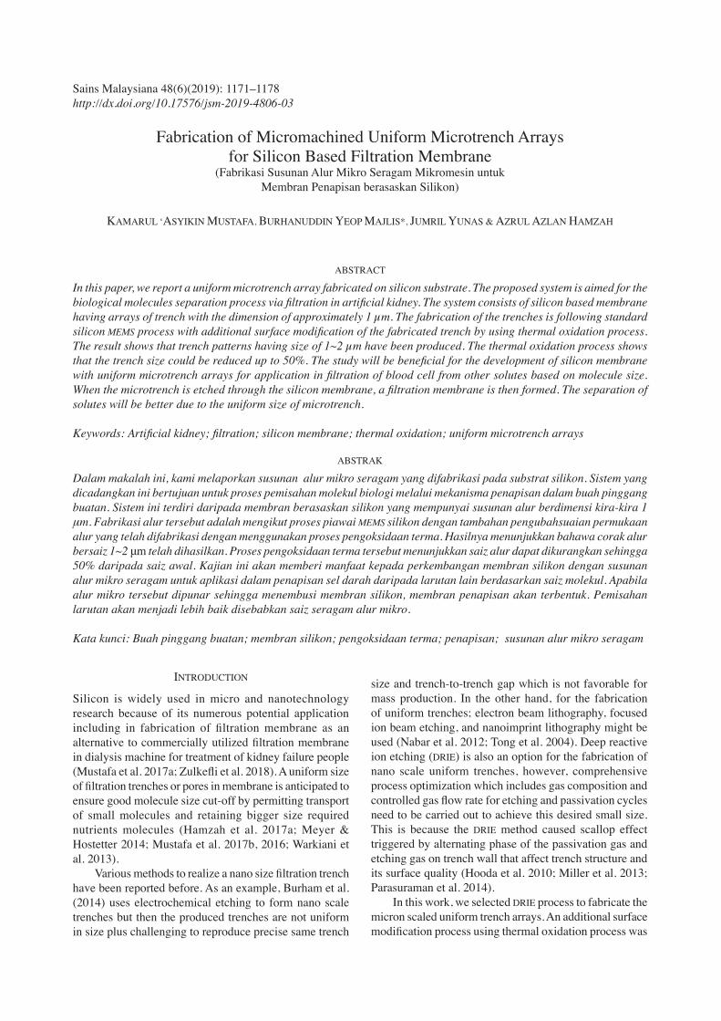
implemented to minimize the scallop effect of the DRIE process at the same time to obtain designed trench size. Thus, the fabrication process of trench arrays is simpler while a controlled size of trench arrays structure still could be produced. By fabricating only microtrench instead of nanotrench arrays, time and cost for process optimization could be reduced. The size of the microtrench could then be further reduced using thermal dry oxidation process which is conducted following the DRIE process. Figure 1 illustrates the final silicon based filtration membrane with uniform trench arrays aimed for application in filtration of blood molecules from smaller solute molecules in artificial kidney.
trench gap of 5 μm. The designed pattern is then transferred to a Chrome mask for subsequent uniform trench fabrication processes. For the pattern development on photoresist layer as shown in Figure 2, initially two Microposit’s photoresists; S1805 and S1813 are evaluated to be used as the photolithography pattern transfer mask for the designed microtrench. These photoresists thickness on different rotation per minute (rpm) spun at 40 s are characterized using Dektak surface profiler to determine which one is appropriate to be used for the specified microtrench size. The selected photoresist is then spun at several different rpm to decide for optimal spin coating rpm for the designed microtrench. Obtained photoresist thickness profiles is presented in Figure 5. Afterwards, using selected photoresist based on photoresist thickness profile conducted earlier, the silicon substrate is spin-coated at the decided optimal rpm. The spin-coated photoresist layer is then exposed to UV light during photolithography process to transfer pattern in Chrome mask. Following the photoresist spin-coating process, photoresist soft bake process is conducted at 115°C for 90 s on a hot plate. Later, the prepared substrate is ready for pattern transfer by photolithography using Midas mask aligner. The substrate is exposed to UV light for 15 s, and then the microtrench pattern is developed in AZ726MIF developer. Once the microtrench pattern is fully developed, the substrate is rinsed with DI water and blow dried with nitrogen gas before it is subjected to post bake process at 120°C for 60 s to harden the photoresist before ready for subsequent DRIE process. Table 1 shows the pattern transfer process parameter characterization conducted for the fabrication process optimization of uniform silicon microtrench. From the characterization conducted for both S1805 and S1813 photoresist, S1813 is selected due to characteristic
FIGURE 1. Blood filtration concept (trench size and counts are not to scale)
MATERIALS AND METHODS
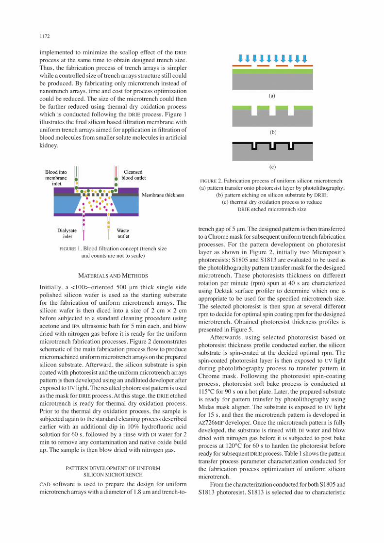
Initially, a <100>-oriented 500 μm thick single side polished silicon wafer is used as the starting substrate for the fabrication of uniform microtrench arrays. The silicon wafer is then diced into a size of 2 cm × 2 cm before subjected to a standard cleaning procedure using acetone and IPA ultrasonic bath for 5 min each, and blow dried with nitrogen gas before it is ready for the uniform microtrench fabrication processes. Figure 2 demonstrates schematic of the main fabrication process flow to produce micromachined uniform microtrench arrays on the prepared silicon substrate. Afterward, the silicon substrate is spin coated with photoresist and the uniform microtrench arrays pattern is then developed using an undiluted developer after exposed to UV light. The resulted photoresist pattern is used as the mask for DRIE process. At this stage, the DRIE etched microtrench is ready for thermal dry oxidation process. Prior to the thermal dry oxidation process, the sample is subjected again to the standard cleaning process described earlier with an additional dip in 10% hydrofluoric acid solution for 60 s, followed by a rinse with DI water for 2 min to remove any contamination and native oxide build up. The sample is then blow dried with nitrogen gas.
PATTERN DEVELOPMENT OF UNIFORM SILICON MICROTRENCH
CAD software is used to prepare the design for uniform microtrench arrays with a diameter of 1.8 μm and trench-to-
FIGURE 2. Fabrication process of uniform silicon microtrench: (a) pattern transfer onto photoresist layer by photolithography;
(b) pattern etching on silicon substrate by DRIE; (c) thermal dry oxidation process to reduce
DRIE etched microtrench size
(a)
(b)
(c)
1173
it offers that will be discussed later on in Results and Discussion section. The optimized fabrication process parameter for S1813 for the purpose of 1.8 μm sized uniform microtrench arrays pattern transfer is summarized in Table 2.
DRIE FOR PATTERN ETCHING OF UNIFORM SILICON MICROTRENCH
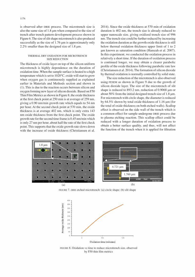
The prepared substrate in the Pattern Development of Uniform Silicon Microtrench section is sent to DRIE process in order to etch the photoresist unprotected silicon area beneath the patterned uniform microtrench array structure on photoresist layer for two minutes to obtain required silicon etch depth. High density reactive ion sulfur hexafluoride (SF6) etching gas is used with passivation gas C4H8 and oxygen at cryogenic temperature. The etched depth of the uniform microtrench structure will be the thickness of silicon membrane of final filtration device once the back end of the substrate is etched later using silicon bulk micromachining technique. The result for DRIE of microtrench is shown in Figure 7 which is analyzed by field emission scanning electron microscopy (FESEM). The FESEM image of circle and slit shape microtrench is observed after photoresist removal once the DRIE process is completed.
THERMAL OXIDATION FOR MICROTRENCH SIZE REDUCTION
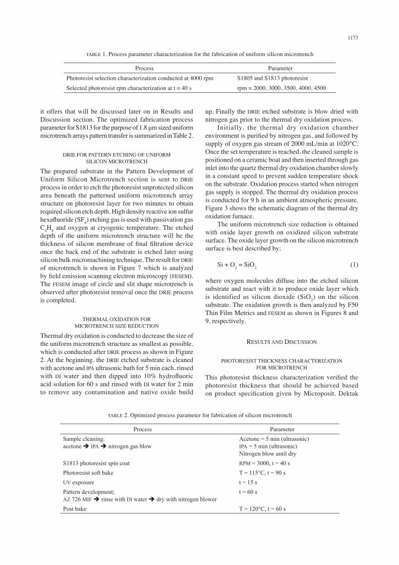
Thermal dry oxidation is conducted to decrease the size of the uniform microtrench structure as smallest as possible, which is conducted after DRIE process as shown in Figure 2. At the beginning, the DRIE etched substrate is cleaned with acetone and IPA ultrasonic bath for 5 min each, rinsed with DI water and then dipped into 10% hydrofluoric acid solution for 60 s and rinsed with DI water for 2 min to remove any contamination and native oxide build
up. Finally the DRIE etched substrate is blow dried with nitrogen gas prior to the thermal dry oxidation process. Initially, the thermal dry oxidation chamber environment is purified by nitrogen gas, and followed by supply of oxygen gas stream of 2000 mL/min at 1020°C. Once the set temperature is reached, the cleaned sample is positioned on a ceramic boat and then inserted through gas inlet into the quartz thermal dry oxidation chamber slowly in a constant speed to prevent sudden temperature shock on the substrate. Oxidation process started when nitrogen gas supply is stopped. The thermal dry oxidation process is conducted for 9 h in an ambient atmospheric pressure. Figure 3 shows the schematic diagram of the thermal dry oxidation furnace. The uniform microtrench size reduction is obtained with oxide layer growth on oxidized silicon substrate surface. The oxide layer growth on the silicon microtrench surface is best described by;
Si + O2 = SiO2 (1)
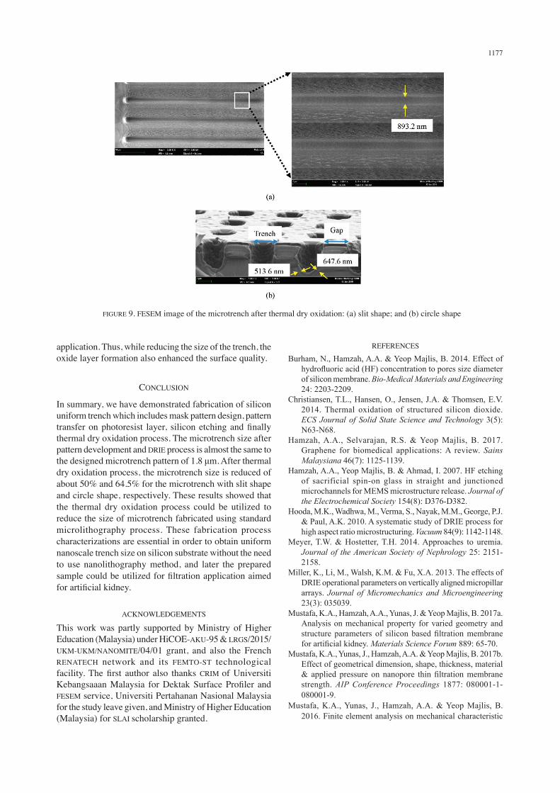
where oxygen molecules diffuse into the etched silicon substrate and react with it to produce oxide layer which is identified as silicon dioxide (SiO2) on the silicon substrate. The oxidation growth is then analyzed by F50 Thin Film Metrics and FESEM as shown in Figures 8 and 9, respectively.
RESULTS AND DISCUSSION
PHOTORESIST THICKNESS CHARACTERIZATION FOR MICROTRENCH
This photoresist thickness characterization verified the photoresist thickness that should be achieved based on product specification given by Microposit. Dektak
TABLE 1. Process parameter characterization for the fabrication of uniform silicon microtrench
Process ParameterPhotoresist selection characterization conducted at 4000 rpm S1805 and S1813 photoresistSelected photoresist rpm characterization at t = 40 s rpm = 2000, 3000, 3500, 4000, 4500
TABLE 2. Optimized process parameter for fabrication of silicon microtrench
Process ParameterSample cleaning: acetone è IPA è nitrogen gas blow
Acetone = 5 min (ultrasonic)IPA = 5 min (ultrasonic)Nitrogen blow until dry
S1813 photoresist spin coat RPM = 3000, t = 40 sPhotoresist soft bake T = 115°C, t = 90 sUV exposure t = 15 sPattern development;AZ 726 MIF è rinse with DI water è dry with nitrogen blower
t = 60 s
Post bake T = 120°C, t = 60 s
1174
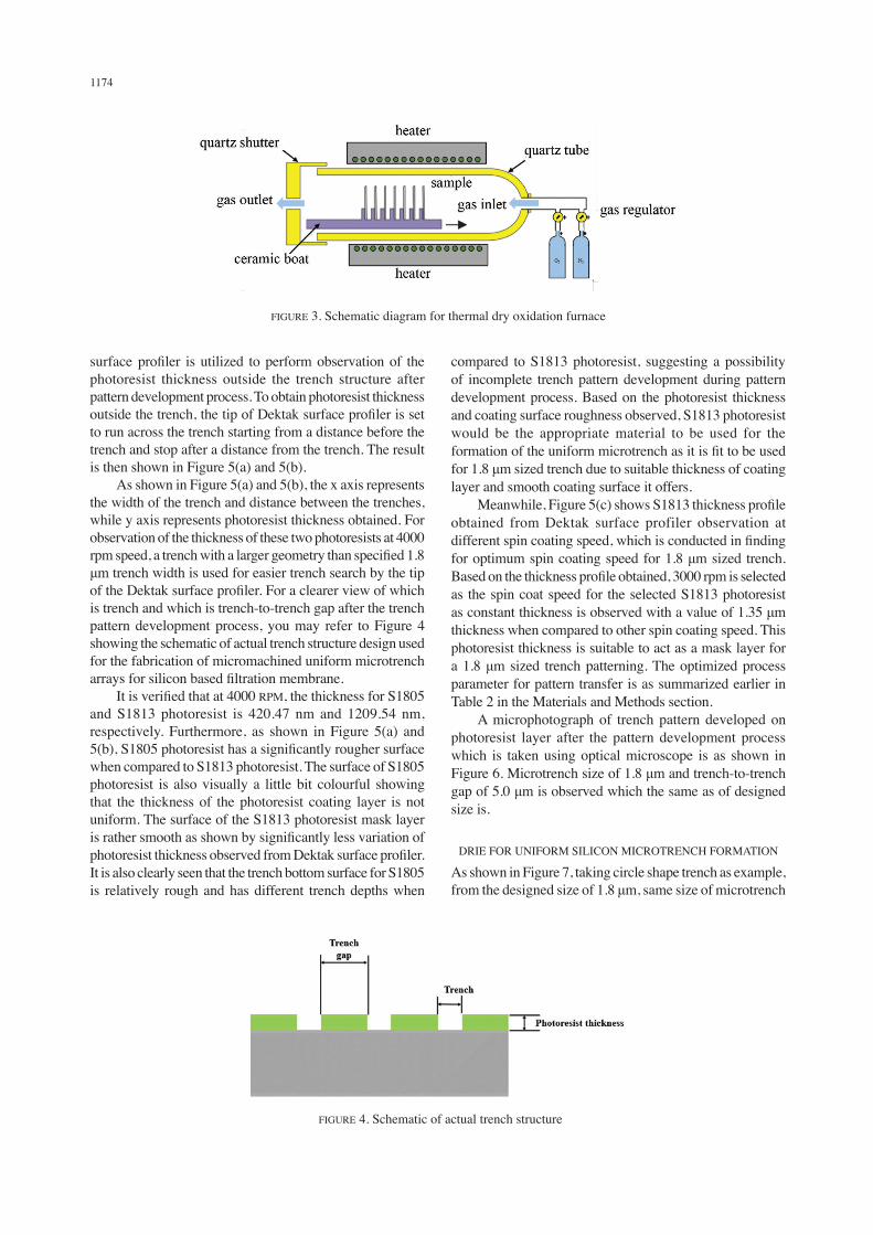
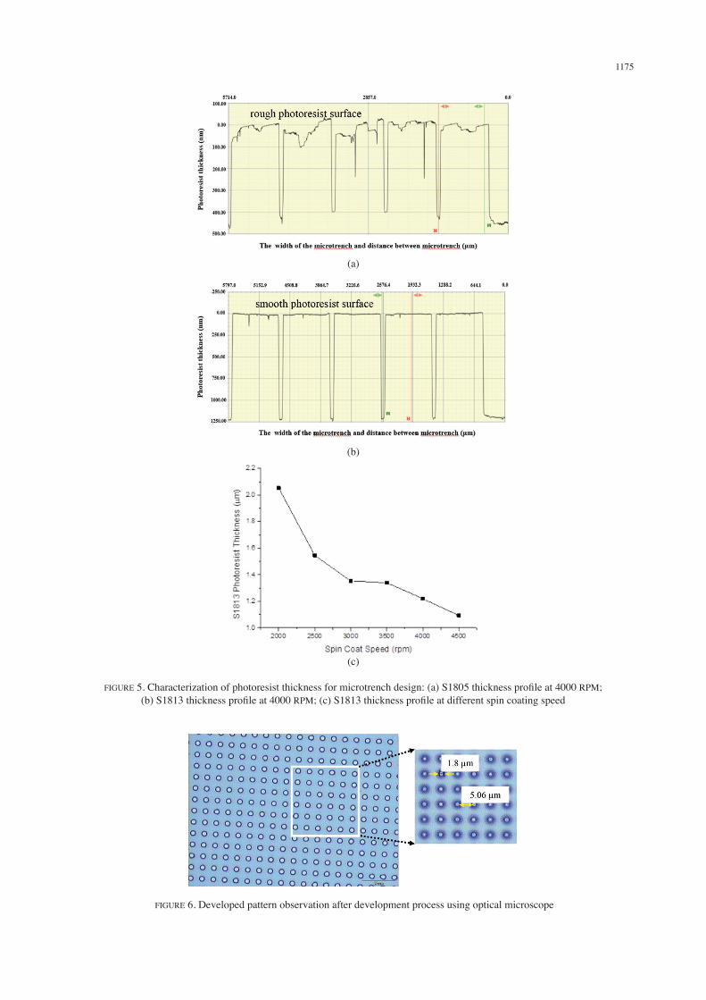
surface profiler is utilized to perform observation of the photoresist thickness outside the trench structure after pattern development process. To obtain photoresist thickness outside the trench, the tip of Dektak surface profiler is set to run across the trench starting from a distance before the trench and stop after a distance from the trench. The result is then shown in Figure 5(a) and 5(b). As shown in Figure 5(a) and 5(b), the x axis represents the width of the trench and distance between the trenches, while y axis represents photoresist thickness obtained. For observation of the thickness of these two photoresists at 4000 rpm speed, a trench with a larger geometry than specified 1.8 μm trench width is used for easier trench search by the tip of the Dektak surface profiler. For a clearer view of which is trench and which is trench-to-trench gap after the trench pattern development process, you may refer to Figure 4 showing the schematic of actual trench structure design used for the fabrication of micromachined uniform microtrench arrays for silicon based filtration membrane. It is verified that at 4000 RPM, the thickness for S1805 and S1813 photoresist is 420.47 nm and 1209.54 nm, respectively. Furthermore, as shown in Figure 5(a) and 5(b), S1805 photoresist has a significantly rougher surface when compared to S1813 photoresist. The surface of S1805 photoresist is also visually a little bit colourful showing that the thickness of the photoresist coating layer is not uniform. The surface of the S1813 photoresist mask layer is rather smooth as shown by significantly less variation of photoresist thickness observed from Dektak surface profiler. It is also clearly seen that the trench bottom surface for S1805 is relatively rough and has different trench depths when
compared to S1813 photoresist, suggesting a possibility of incomplete trench pattern development during pattern development process. Based on the photoresist thickness and coating surface roughness observed, S1813 photoresist would be the appropriate material to be used for the formation of the uniform microtrench as it is fit to be used for 1.8 μm sized trench due to suitable thickness of coating layer and smooth coating surface it offers. Meanwhile, Figure 5(c) shows S1813 thickness profile obtained from Dektak surface profiler observation at different spin coating speed, which is conducted in finding for optimum spin coating speed for 1.8 μm sized trench. Based on the thickness profile obtained, 3000 rpm is selected as the spin coat speed for the selected S1813 photoresist as constant thickness is observed with a value of 1.35 μm thickness when compared to other spin coating speed. This photoresist thickness is suitable to act as a mask layer for a 1.8 μm sized trench patterning. The optimized process parameter for pattern transfer is as summarized earlier in Table 2 in the Materials and Methods section. A microphotograph of trench pattern developed on photoresist layer after the pattern development process which is taken using optical microscope is as shown in Figure 6. Microtrench size of 1.8 μm and trench-to-trench gap of 5.0 μm is observed which the same as of designed size is.
DRIE FOR UNIFORM SILICON MICROTRENCH FORMATION
As shown in Figure 7, taking circle shape trench as example, from the designed size of 1.8 μm, same size of microtrench
FIGURE 3. Schematic diagram for thermal dry oxidation furnace
FIGURE 4. Schematic of actual trench structure
1175
FIGURE 6. Developed pattern observation after development process using optical microscope
FIGURE 5. Characterization of photoresist thickness for microtrench design: (a) S1805 thickness profile at 4000 RPM; (b) S1813 thickness profile at 4000 RPM; (c) S1813 thickness profile at different spin coating speed
(a)
(b)
(c)
1176
is observed after DRIE process. The microtrench size is also the same size of 1.8 μm when compared to the size of trench after trench pattern development process shown in Figure 6. The size of slit shape microtrench is also produced successfully as the size of 1.76 μm is approximately only 2.2% smaller than the designed size of 1.8 μm.
THERMAL DRY OXIDATION FOR MICROTRENCH SIZE REDUCTION
The thickness of oxide layer on top of the silicon uniform microtrench is highly dependence on the duration of oxidation time. When the sample surface is heated to a high temperature which is set to 1020°C, oxide will start to grow when oxygen gas is continuously supplied as explained earlier in Materials and Methods section and shown in (1). This is due to the reaction occurs between silicon and oxygen forming new layer of silicon dioxide. Based on F50 Thin Film Metrics as shown in Figure 8, the oxide thickness at the first check point at 250 min is at average of 259 nm, giving a 0.90 nm/min growth rate which equals to 54 nm per hour. At the second check point at 570 min, the oxide thickness is at average 402 nm, which is only extra 143 nm oxide thickness from the first check point. The oxide growth rate for the second time frame is 0.45 nm/min which is only 27 nm per hour, about half the rate of the first check point. This supports that the oxide growth rate slows down with the increase of oxide thickness (Christiansen et al.
2014). Since the oxide thickness at 570 min of oxidation duration is 402 nm, the trench size is already reduced to upper nanoscale size, giving oxidized trench size of 996 nm. The trench size could be further reduced by increasing the oxidation duration as the growth oxide thickness is still below thermal oxidation thickness upper limit of 1 to 2 μm known as saturation condition (Hamzah et al. 2007). In this experiment, we conducted the oxidation process in relatively a short time. If the duration of oxidation process is continued longer, we may obtain a clearer parabolic profile of the oxide thickness following parabolic rate law (Christiansen et al. 2014). The formation of silicon dioxide by thermal oxidation is normally controlled by solid state. The size reduction of the microtrench is also observed using FESEM as shown in Figure 9 due to the growth of silicon dioxide layer. The size of the microtrench of slit shape is reduced to 893.2 nm, reduction of 0.9068 μm or about 50% from the initial designed trench size of 1.8 μm. For microtrench with circle shape, the diameter is reduced by 64.5% shown by total oxide thickness of 1.16 μm (for the total of oxide thickness on both etched walls). Scallop effect is observed on the side wall of the trench which is a common effect for sample undergone DRIE process due to plasma etching reaction. This scallop effect could be reduced with a longer duration of oxidation process to obtain a better surface quality, and thus, will not affect the function of the trench when it is applied for filtration
FIGURE 8. Oxidation vs time to reduce microtrench size, observed by F50 thin film metrics
FIGURE 7. DRIE etched microtrench: (a) circle shape; (b) slit shape
1.8 μm
(a) (b)
4.721 μm
1.760 μm
1177
application. Thus, while reducing the size of the trench, the oxide layer formation also enhanced the surface quality.
CONCLUSION
In summary, we have demonstrated fabrication of silicon uniform trench which includes mask pattern design, pattern transfer on photoresist layer, silicon etching and finally thermal dry oxidation process. The microtrench size after pattern development and DRIE process is almost the same to the designed microtrench pattern of 1.8 μm. After thermal dry oxidation process, the microtrench size is reduced of about 50% and 64.5% for the microtrench with slit shape and circle shape, respectively. These results showed that the thermal dry oxidation process could be utilized to reduce the size of microtrench fabricated using standard microlithography process. These fabrication process characterizations are essential in order to obtain uniform nanoscale trench size on silicon substrate without the need to use nanolithography method, and later the prepared sample could be utilized for filtration application aimed for artificial kidney.
ACKNOWLEDGEMENTS
This work was partly supported by Ministry of Higher Education (Malaysia) under HiCOE-AKU-95 & LRGS/2015/UKM-UKM/NANOMITE/04/01 grant, and also the French RENATECH network and its FEMTO-ST technological facility. The first author also thanks CRIM of Universiti Kebangsaaan Malaysia for Dektak Surface Profiler and FESEM service, Universiti Pertahanan Nasional Malaysia for the study leave given, and Ministry of Higher Education (Malaysia) for SLAI scholarship granted.
REFERENCES
Burham, N., Hamzah, A.A. & Yeop Majlis, B. 2014. Effect of hydrofluoric acid (HF) concentration to pores size diameter of silicon membrane. Bio-Medical Materials and Engineering 24: 2203-2209.
Christiansen, T.L., Hansen, O., Jensen, J.A. & Thomsen, E.V. 2014. Thermal oxidation of structured silicon dioxide. ECS Journal of Solid State Science and Technology 3(5): N63-N68.
Hamzah, A.A., Selvarajan, R.S. & Yeop Majlis, B. 2017. Graphene for biomedical applications: A review. Sains Malaysiana 46(7): 1125-1139.
Hamzah, A.A., Yeop Majlis, B. & Ahmad, I. 2007. HF etching of sacrificial spin-on glass in straight and junctioned microchannels for MEMS microstructure release. Journal of the Electrochemical Society 154(8): D376-D382.
Hooda, M.K., Wadhwa, M., Verma, S., Nayak, M.M., George, P.J. & Paul, A.K. 2010. A systematic study of DRIE process for high aspect ratio microstructuring. Vacuum 84(9): 1142-1148.
Meyer, T.W. & Hostetter, T.H. 2014. Approaches to uremia. Journal of the American Society of Nephrology 25: 2151-2158.
Miller, K., Li, M., Walsh, K.M. & Fu, X.A. 2013. The effects of DRIE operational parameters on vertically aligned micropillar arrays. Journal of Micromechanics and Microengineering 23(3): 035039.
Mustafa, K.A., Hamzah, A.A., Yunas, J. & Yeop Majlis, B. 2017a. Analysis on mechanical property for varied geometry and structure parameters of silicon based filtration membrane for artificial kidney. Materials Science Forum 889: 65-70.
Mustafa, K.A., Yunas, J., Hamzah, A.A. & Yeop Majlis, B. 2017b. Effect of geometrical dimension, shape, thickness, material & applied pressure on nanopore thin filtration membrane strength. AIP Conference Proceedings 1877: 080001-1-080001-9.
Mustafa, K.A., Yunas, J., Hamzah, A.A. & Yeop Majlis, B. 2016. Finite element analysis on mechanical characteristic
FIGURE 9. FESEM image of the microtrench after thermal dry oxidation: (a) slit shape; and (b) circle shape

1178
of nanoslit filtration membrane for artificial kidney. International Conference in Semiconductor Electronics. pp. 21-24.
Nabar, B.P., Çelik-Butler, Z., Dennis, B.H. & Billo, R.E. 2012. A nanoporous silicon nitride membrane using a two-step lift-off pattern transfer with thermal nanoimprint lithography. Journal of Micromechanics and Microengineering 22(4): 045012.
Parasuraman, J., Summanwar, A., Marty, F., Basset, P., Angelescu, D.E. & Bourouina, T. 2014. Microelectronic engineering deep reactive ion etching of sub-micrometer trenches with ultra high aspect ratio. Microelectronic Engineering 113: 35-39.
Tong, H.D., Jansen, H.V., Gadgil, V.J., Bostan, C.G., Berenschot, E., Van Rijn, C.J.M. & Elwenspoek, M. 2004. Silicon nitride nanosieve membrane. Nano Letters 4(2): 283-287.
Warkiani, M.E., Bhagat, A.A.S., Khoo, B.L., Han, J., Lim, C.T., Gong, H.Q. & Fane, A.G. 2013. Isoporous micro/nanoengineered membranes. ACS Nano 7(3): 1882-1904.
Zulkefli, M.A., Mohamed, M.A., Siow, K.S. & Yeop Majlis, B. 2018. Nanoelectromechanical system switching devices (NEMS) based on graphine and carbon nano tube (CNT). Sains Malaysiana 47(3): 619-633.
Kamarul ‘Asyikin Mustafa, Burhanuddin Yeop Majlis*, Jumril Yunas & Azrul Azlan HamzahInstitute of Microengineering and NanoelectronicsUniversiti Kebangsaan Malaysia43600 UKM Bangi, Selangor Darul EhsanMalaysia
Kamarul ‘Asyikin MustafaDepartment of Electrical and Electronics Engineering Faculty of EngineeringUniversiti Pertahanan Nasional Malaysia57000 Sungai Besi, Kuala Lumpur, Federal TerritoryMalaysia
*Corresponding author; email: [email protected]
Received: 16 July 2018Accepted: 21 January 2019