7271606 spring based probe pin that allo
TRANSCRIPT
8/4/2019 7271606 Spring Based Probe Pin That Allo
http://slidepdf.com/reader/full/7271606-spring-based-probe-pin-that-allo 1/9
(12) United States PatentTang et al.
(54) SPRING-BASED PROBE PIN THAT ALLOWS
KELVIN TESTING
(75) Inventors: Tze Kang Tang, Melaka (MY); SekHoi Chong, Melaka (MY); Chin Chai
Gan, Melaka (MY); Hai Ching Tan,
Melaka (MY)
(73) Assignee: National Semiconductor Corporation,
Santa Clara, CA (US)
( *) Notice: Subject to any disclaimer, the term of this
patent is extended or adjusted under 35
U.S.c. 154(b) by 0 days.
(21) Appl. No.: 111197,916
(22) Filed: Aug. 4, 2005
(51) Int. Cl.G01R 31102 (2006.01)
G01R 27108 (2006.01)
G01R 31128 (2006.01)
(52) U.S. Cl. ...................... 3241761; 324/715; 3241754;
3241158.1
(58) Field of Classification Search ................ 3241754,
3241755,715,761, 158.1
See application file for com plete search history.
(56) References Cited
U.S. PATENT DOCUMENTS
4,027 935 A * 611977 Byrnes et al. ...... ...... .. 4391289
516C
D
E1
526S2 _ - - - 1 ~ 526S1
526S3526S4-
E2----.JL....o<
514A
512
515
111111 1111111111111111111111111111111111111111111111111111111111111US007271606Bl
(10) Patent No.: US 7,271,606 BlSep.18,200745) Date of Patent:
4,622,514 A *
4,764,026 A *
5,500,605 A *
5,641,945 A6,150,830 A *
6,257,911 Bl
6,291,897 Bl *
6,411,112 Bl *6,462,572 B2 *
6,471,524 Bl *
6,530,148 Bl *
6,552,554 Bl *
6,714,029 B2
6,768,331 B2
6,791,344 B2 *
2005/0179455 Al *
* cited by examiner
1111986 Lewis ........................ 3241761
8/1988 Powell et al. ............... 374/178
3/1996 Chang ........................ 3241758
6/1997 Abe et al .................... 174/2611112000 Schmid et al. ...... ...... .. 3241761
7/2001 Shelby et al. ........ ....... 4391268
912001 Wark et al. ................. 2571786
6/2002 Das et al. ................... 3241754
1012002 Takahashi ................... 3241755
1012002 Nakano et al ................ 439170
3/2003 Kister .. ... ... ... ..... ... ... ... 29/842
412003 Prinz et al. ................. 3241719
3/2004 Prasad-Roth ................ 3241754
7/2004 Longson et al ............. 3241761
912004 Cook et al. ................. 3241754
8/2005 Cooper et al. .............. 3241754
PrimaryExaminer-Ernest
KarlsenAssistant Examiner-Roberto Velez
(74) Attorney, Agent, or Firm-Mark C. Pickering
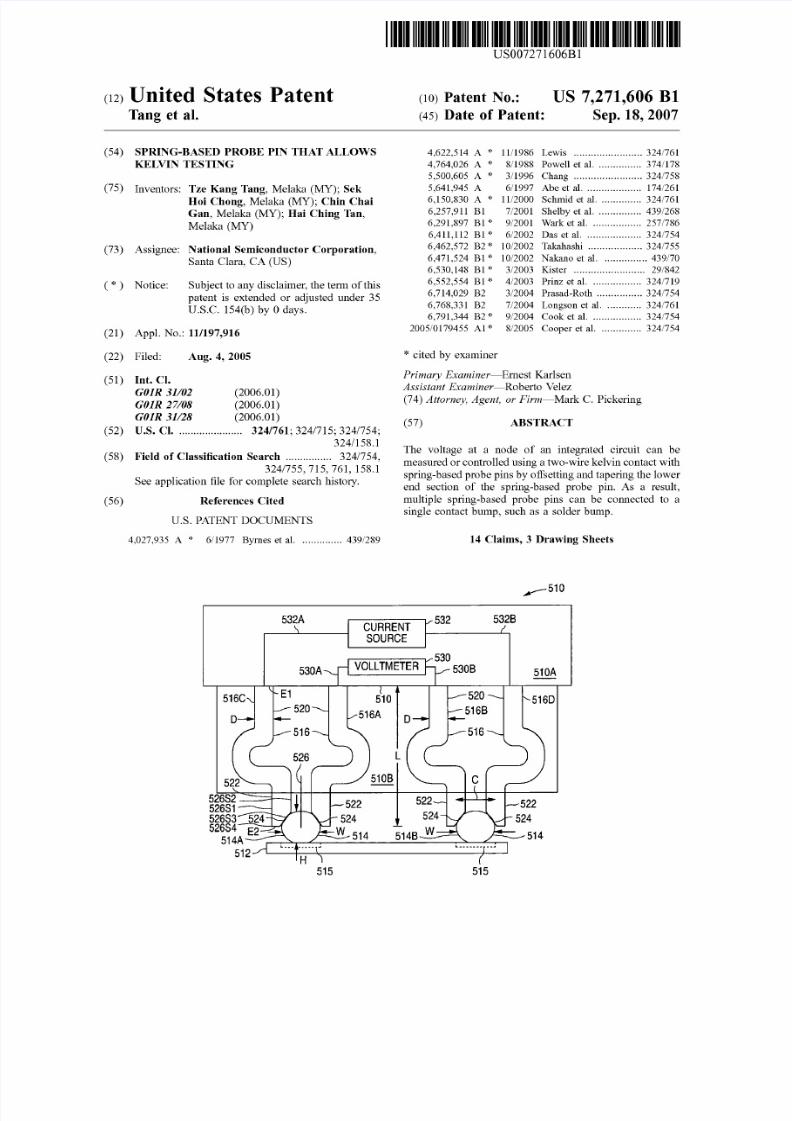
(57) ABSTRACT
The voltage at a node of an integrated circuit can be
measured or controlled using a two-wire kelvin contact with
spring-based probe pins by offsetting and tapering the low er
end section of the spring-based probe pin. As a result,
multiple spring-based probe pins can be connected to a
single contact bump, such as a solder bump.
14 Claims, 3 Drawing Sheets
520
5168
515
5328
;---510
510A
516D
514
8/4/2019 7271606 Spring Based Probe Pin That Allo
http://slidepdf.com/reader/full/7271606-spring-based-probe-pin-that-allo 2/9
u.s. Patent Sep.18,2007 Sheet 1 of 3 US 7,271,606 Bl
114
, 1 00
110
112
FIG. 1(PRIOR ART)
IN I
I
Y
I
I
216
310(
DEVICE
312(
VOLTMETER
3)4
CURRENT
SOURCE
FIG. 3(PRIOR ART)
220
222
224
214
/ 210
210A
FIG. 2(PRIOR ART)
, -300
OUT
f-
8/4/2019 7271606 Spring Based Probe Pin That Allo
http://slidepdf.com/reader/full/7271606-spring-based-probe-pin-that-allo 3/9
u.s. Patent Sep.18,2007
4 0 0 ,
515
Sheet 2 of 3
412
416
FIG. 4
CURRENT
SOURCE
FIG. 5
414
520
516B
516
C
515
532B
US 7,271,606 Bl
.;---510
510A
516D
522
8/4/2019 7271606 Spring Based Probe Pin That Allo
http://slidepdf.com/reader/full/7271606-spring-based-probe-pin-that-allo 4/9
u.s. Patent
618
626
612
615
Sep.18,2007 Sheet 3 of 3
614
618
626
615
FIG. 6
~ 6 1 0 610A
620
615
A N
FIG. 7
US 7,271,606 Bl
8/4/2019 7271606 Spring Based Probe Pin That Allo
http://slidepdf.com/reader/full/7271606-spring-based-probe-pin-that-allo 5/9
US 7,271,606 Bl
1SPRING-BASED PROBE PIN THAT ALLOWS
KELVIN TESTING
BACKGROUND OF THE INVENTION
1. Field of the Invention
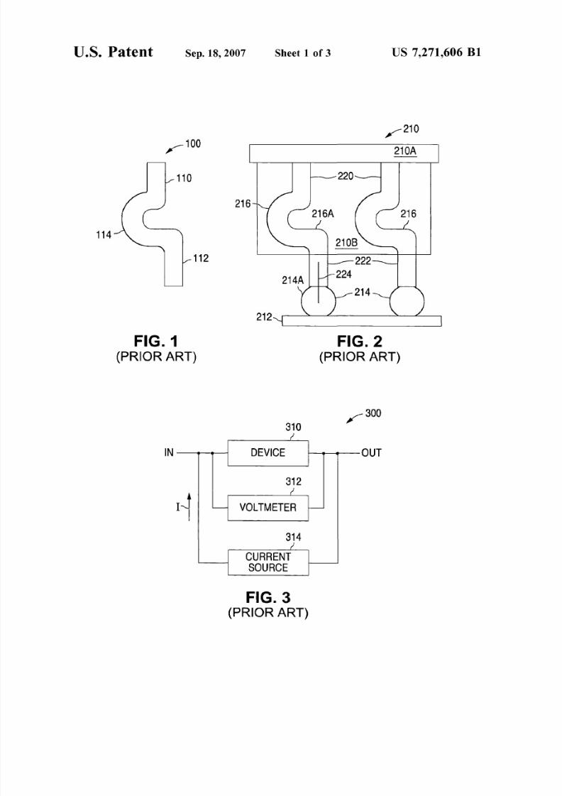
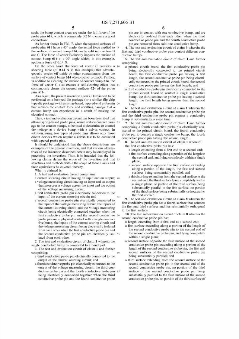
2FIG. 3 shows a bl ock diagram that illustrates an example
of a prior-art kelvin test apparatus 300, used to measu re the
impedance of device 310. As shown in FIG. 3, apparatus 300
includes a device 310, such as a winding, which has an input
IN and an output OUT. In addition, apparatus 300 has a
voltmeter 312 and a current source 314 that are connected
between the input IN and the output OUT of device 310.he present invention relates to probe pins and, more
particularly, to a spring-based probe pin that allows kelvin
testing.
2. Description of the Related Art
In operation, to measure device 310, a test current I is
passed through device 310, and the resulting voltage pro-
10 duced across device 310 is measured. A kelvin test allows
A bumped die package is a package that eliminates the
need for wire bonding and molding. With a bumped die
process, solder bumps are mounted to the bond pads of a
wafer, which is then diced to form a large number of
individual die. Once diced, an individual die is ready to be 15
used by a customer.
Final electrical testing is performed using a test and
evaluation circuit that includes a number of probe pins. In
operation, the probe pins are brought into electrical contact
with the solder bumps. Voltages and currents are then 20
applied to the solder bumps via the probe pins so that the
proper operation of the circuits can be verified.
In current-generation test and evaluation circuits, the
probe pins are commonly implemented as pogo pins or 25
cantilever pins. A pogo pin is typically implemented as a
cylindrically-shaped structure that houses a spring, alth ough
other types of spring-based probe pins can alternately be
used.
the voltage to be accurately measured because the imped
ance of voltmeter 312 is very high (effectively allowing the
lead-line and contact resistance to be neglected). The imped-
ance of device 310 can then be determined by dividing the
voltage by the current.
Thus, to perform a kelvin test on a bumped die package,
two separate contacts must be made with a solder bump: one
to provide current and one to measure voltage. S ince spring
based probe pins are axially aligned with the solder bumps
to contact the apexes of the solder bumps, it is not possible
for two conventional spring-based probe pins to make an
electrical connection with a single solder bump without
severely damaging the solder bump.Cantilever pins, on the other hand, are not axially aligned
with the solder bumps on the bumped die package. Instead,
cantilever pins approach the solder bumps from the side. As
a result, a pair of cantilever pins can be used to contact a
single solder bump, thereby allowing a kelvin test to be
performed.
One disadvantage of cantilever pins, however, is that the
cantilever pins can significantly damage the solder bumps
when the cantilever pins and solder bumps are brought into
contact. Since cantilever pins approach the solder bumps
from the side, it is not uncommon for a cantilever pin to first
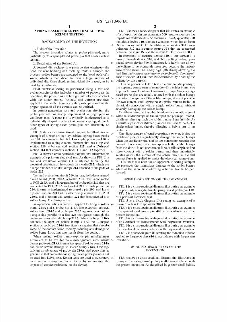
FIG. 1 shows a cross-sectional diagram that illustrates an 30
example of a prior-art, non-cylindrical, spring-based probe
pin 100. As shown in the FIG. 1 example, probe pin 100 is
implemented as a single metal element that has a top end
section 110, a bottom end section 112, and a C-shaped
section 114 that connects sections 110 and 112 together.35 make contact with a solder bump, and then undesirably
scratch across the surface of the solder bump as the full
contact force is applied to make the electrical connection.
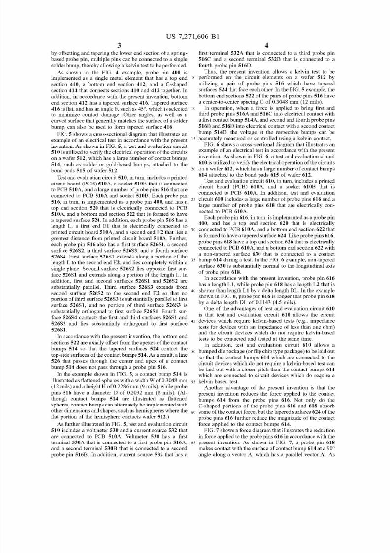
FIG. 2 shows a cross-sectional diagram that illustrates an
example of a prior-art electrical test. As shown in FIG. 2, a
test and evaluation circuit 210 is utilized to verify the
electrical operation of the circuits on a wafer 212, which has
a large number of solder bumps 214 attached to the pads of
wafer 212.
Thus, there is a need for an approach to testing bumpeddie packages that minimizes damage to the solder bumps
40 while at the same time allowing a kelvin test to be per-
Test and evaluation circuit 210, in turn, includes a printed
circuit board (PCB) 210A, a socket 210B that is connected
to PCB 210A, an d a large number of probe pins 216 that are
connected to PCB 210A and socket 210B. Each probe pin 45
216, in turn, is implemented as a probe pin 100, and has a
top end section 220 that is electrically connected to PCB
210A, and a bottom end section 222 that is connected to a
solder bump 214 during a test.
In operation, when a force is applied to bring a solder 50
bump 214A and a probe pin 216A into electrical contact,
solder bump 214A and probe pin 216A approach each other
along a line parallel to a line 224 that passes through the
center and apex of solder bump 214A. When probe pin 216Acontacts the apex of solder bump 214A, the C-shaped 55
section of probe pin 216A functions as a spring that absorbs
some of the contact force, thereby reducing any damage to
solder bump 214A that may result from the contact.
formed.
BRIEF DESCRIPTION OF THE DRAWINGS
FIG. 1 is a cross-sectional diagram illustrating an example
of a prior-art, non-cylindrical, spring-based probe pin 100.
FIG. 2 is a cross-sectional diagram illustrating an example
of a prior-art electrical test.
FIG. 3 is a block diagram illustrating an example of a
prior-art kelvin test apparatus 300.
FIG. 4 is a cross-sectional diagram illustrating an example
of a spring-based probe pin 400 in accordance with the
present invention.
FIG. 5 is a cross-sectional diagram illustrating an exampleof an electrical test in accordance wi th the present invention.
FIG. 6 is a cross-sectional diagram illustrating an example
of an electrical test in accordance wi th the present invention.
FIG. 7 is a force diagram illustrating the reduction in force
applied to the probe pins 616 in accordance with the presenthen testing, solder bump-to-probe pin misaligument
errors are to be avoided as a misaligument error which
causes probe pin 216Ato miss the apex of solder bump 214A
can cause severe damage to solder bump 214A. One sig
nificant disadvantage of probe pin 216A, and pogo pins in
general, is that conventional spring-based probe pins can not
60 invention.
be used in a kelvin test. Kelvin tests are used to accurately 65
measure the voltage across a device by minimizing the
impact of contact resistance on the device.
DETAILED DESCRIPTION OF THE
INVENTION
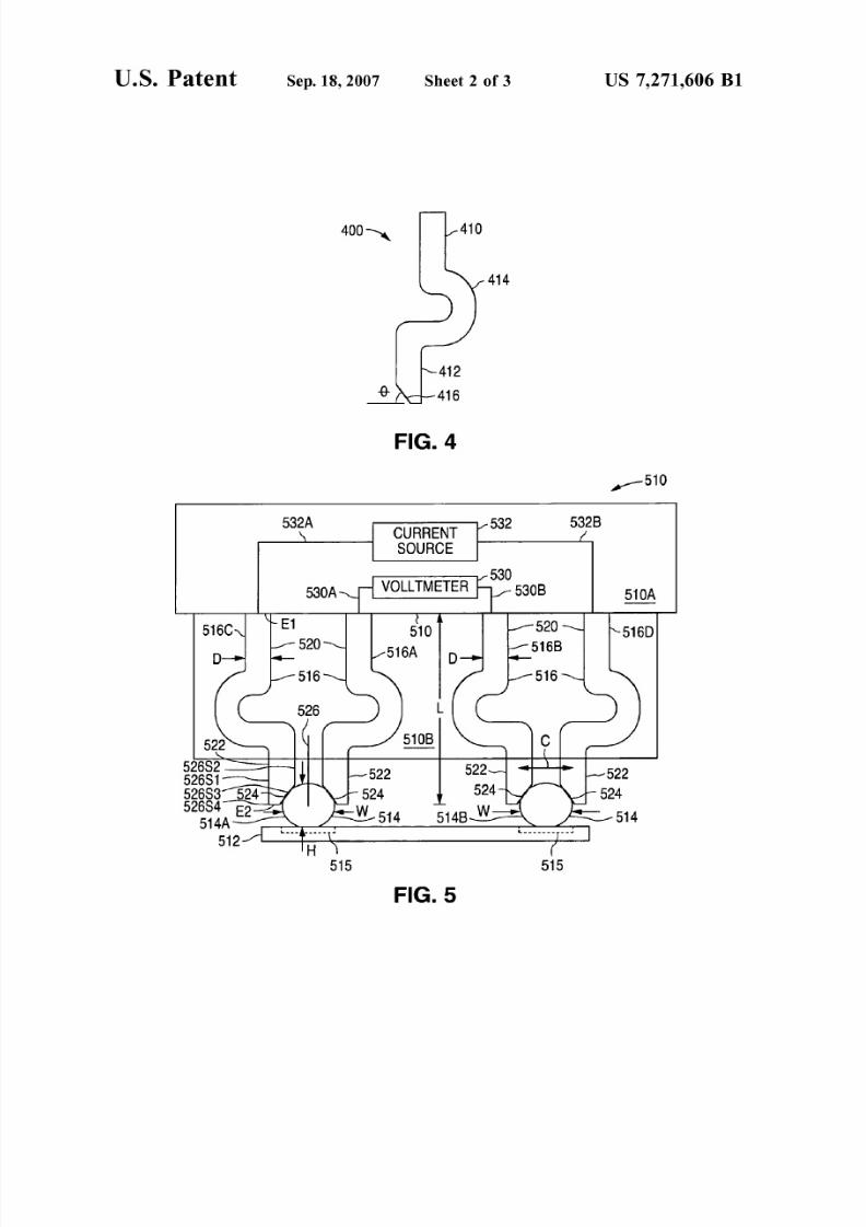
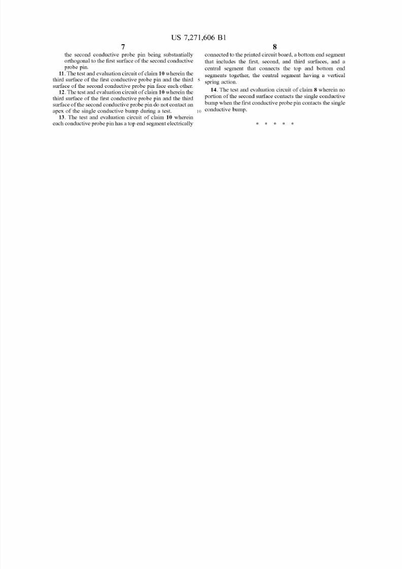
FIG. 4 shows a cross-sectional diagram that illustrates an
example of a spring-based probe pin 400 in accordance with
the present invention. As described in greater detail below,
8/4/2019 7271606 Spring Based Probe Pin That Allo
http://slidepdf.com/reader/full/7271606-spring-based-probe-pin-that-allo 6/9
US 7,271,606 Bl
3by offsetting and tapering the lower end section of a spring
based probe pin, multiple pins can be connected to a single
solder bump, thereby allowing a kelvin test to be performed.
As shown in the FIG. 4 example, probe pin 400 isimplemented as a single metal element that has a top end 5
section 410, a bottom end section 412, and a C-shaped
section 414 that connects sections 410 and 412 together. Inaddition, in accordance with the present invention, bottom
end section 412 has a tapered surface 416. Tapered surface416 is flat, and has an angle 8, such as 45°, which is selected 10
to minimize contact damage. Other angles, as well as a
curved surface that generally matches the surface of a solder
bump, can also be used to fonn tapered surface 416.
4first terminal 532A that is connected to a third probe pin
516C and a second tenninal 532B that is connected to a
fourth probe pin 516D.
Thus, the present invention allows a kelvin test to be
perfonned on the circuit elements on a wafer 512 by
utilizing a pair of probe pins 516 which have tapered
surfaces 524 that face each other. In the FIG. 5 example, the
bottom end sections 522 of the pairs of probe pins 516 have
a center-to-center spacing C of 0.3048 mm (12 mils).
In operation, when a force is applied to bring first and
third probe pins 516A and 516C into electrical contact with
a first contact bump 514A, and second and fourth probe pins
516B and 516D into electrical contact with a second contact
bump 514B, the voltage at the respective bumps can beFIG. 5 shows a cross-sectional diagram that illustrates an
example of an electrical test in accordance with the present
invention. As shown in FIG. 5, a test and evaluation circuit
510 is util ized to verifY the electrical operation of he circuits
15 accurately measured or controlled using a kelv in contact.
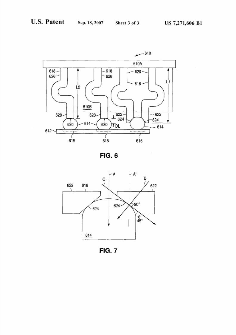
FIG. 6 shows a cross-sectional diagram that illustrates an
example of an electrical test in accordance with the present
invention. As shown in FIG. 6, a test and evaluation circuit
610 is utilized to verifY the electrical operation of he circuitson a wafer 512, which has a large number of contact bumps
514, such as solder or gold-based bumps, attached to the
bond pads 515 of wafer 512.
Test and evaluation circuit 510, in turn, includes a printed
circuit board (PCB) 510A, a socket SlOB that is connected
20 on a wafer 612, which has a large number of contact bumps
614 attached to the bond pads 615 of wafer 612.
to PCB 510A, and a large number of probe pins 516 that are
connected to PCB 510A and socket SlOB. Each probe p in
516, in turn, is implemented as a probe pin 400, and has a
top end section 520 that is electrically connected to PCB
510A, and a bottom end section 522 that is formed to have
Test and evaluation circuit 610, in turn, includes a printed
circuit board (PCB) 610A, and a socket 610B that isconnected to PCB 610A. In addition, test and evaluation
25 circuit 610 includes a large number of probe pins 616 and a
large number of probe pins 618 that are electrically con
nected to PCB 610A.
a tapered surface 524. In addition, each probe pin 516 has a
length L, a first end E1 that is electrically connected toprinted circuit board 510A, and a second end E2 that lies a 30
greatest distance from printed circuit board 510A. Further,
each probe pin 516 also has a first surface 526S1, a second
surface 526S2, a third surface 526S3, and a fourth surface
526S4. First surface 526S1 extends along a portion of the
length L to the second end E2, and lies completely within a 35
single plane. Second surface 526S2 lies opposite first sur
face 526S1 and extends along a portion of the length L. In
addition, first and second surfaces 526S1 and 526S2 aresubstantially parallel. Third surface 526S3 extends from
second surface 526S2 to the second end E2 so that no 40
portion of hird surface 526S3 is substantially parallel to first
surface 526S1, and no portion of third surface 526S3 is
substantially orthogonal to first surface 526Sl. Fourth sur
face 526S4 contacts the first and third surfaces 526S1 and
526S3 and lies substantially orthogonal to first surface 45
526Sl.
In accordance with the present invention, the bottom end
sections 522 are axially offset from the apexes of the contact
bumps 514 so that the tapered surfaces 524 contact the 50
top-side surfaces of he contact bumps 514. As a result, a line
526 that passes through the center and apex of a contact
bump 514 does not pass through a probe pin 516.
Each probe pin 616, in turn, is implemented as a probe pin
400, and has a top end section 620 that is electrically
connected to PCB 610A, and a bottom end section 622 that
is fonned to have a tapered surface 624. Like probe pins 616,
probe pins 618 have a top end section 626 that is electrically
connected to PCB 610A, and a bottom end section 622 with
a non-tapered surface 630 that is connected to a contact
bump 614 during a test. In the FIG. 6 example, non-tapered
surface 630 is substantially nonnal to the longitudinal axis
of probe pins 618.
In accordance with the present invention, probe pin 616has a length L1, while probe pin 618 has a length L2 that is
shorter than length L1 by a delta length DL. In the example
shown in FIG. 6, probe pin 616 is longer that probe pin 618
by a delta length DL of 0.1143 (4.5 mils).
One of the advantages of test and evaluation circuit 610
is that test and evaluation circuit 610 allows the circuit
devices which require kelvin-based tests (e.g., impedance
tests for devices with an impedance of less than one ohm)
and the circuit devices which do not require kelvin-based
tests to be contacted and tested at the same time.
In addition, test and evaluation circuit 610 allows a
bumped die package (or flip chip type package) to be laid out
so that the contact bumps 614 which are connected to the
circuit devices which do not require a kelvin-based test can
be laid out with a closer pitch than the contact bumps 614
which are connected to circuit devices which do require a
55 kelvin-based test.
In the example shown in FIG. 5, a contact bump 514 isillustrated as flattened spheres with a width W of 0.3048 mm
(12 mils) and a height H of 0.2286 mm (9 mils), while probe
pins 516 have a diameter D of 0.2032 mm (8 mils). (Al
though contact bumps 514 are illustrated as flattened
spheres, contact bumps can alternately be implemented with
other dimensions and shapes, such as hemispheres where the 60
flat portion of the hemisphere contacts wafer 512.)
As further illustrated in FIG. 5, test and evaluation circuit
510 includes a voltmeter 530 and a current source 532 that
are connected to PCB 510A. Voltmeter 530 has a first
terminal 530A that is connected to a first probe pin 516A, 65
and a second terminal 530B that is connected to a second
probe pin 516B. In addition, current source 532 that has a
Another advantage of the present invention is that the
present invention reduces the force applied to the contact
bumps 614 from the probe pins 616. Not only do the
C-shaped portions of the probe pins 616 and 618 absorb
some of he contact force, but the tapered surfaces 624 of he
probe pins 616 further reduce the magnitude of the contact
force applied to the contact bumps 614.
FIG. 7 shows a force diagram that illustrates the reduction
in force applied to the probe pins 616 in accordance with the
present invention. As shown in FIG. 7, a probe pin 618
makes contact with the surface of contact bump 614 at a 90°
angle along a vector A, which has a parallel vector A'. As
8/4/2019 7271606 Spring Based Probe Pin That Allo
http://slidepdf.com/reader/full/7271606-spring-based-probe-pin-that-allo 7/9
US 7,271,606 Bl5
such, the bump contact areas are u nder the full force of the
probe pins 618, which is connnonly 0.2 N to ensure a good
connection.
As further shown in FIG. 7, when the tapered surfaces of
probe pins 616 have a 45° angle, the actual force applied to
the surface of contact bump 614 can be split into vectors B
and C. The force of vector B directly impacts the surface of
contact bump 614 at a 90° angle which, in this example,
applies a force of 0.14 N.
On the other hand, the force of vector C provides a 10
sheering force (of 0.14 N in this example) that advanta
geously scrubs off oxide or other contaminants from the
surface of contact bump 614 when contact is made. Further,
in addition to cleaning the surface of contact bump 614, the
force of vector C also creates a self-cleaning effect that 15
continuously cleans the tapered surfaces 624 of the probe
pins 616.
As a result, the present invention allows a kel vin test to be
performed on a bumped die package (or a similar flip chip
type die package) wit h a spring-based, tapered-end pro be pin 20
that reduces the contact force and resulting damage that a
contact bump can experience as a result of making the
electrical contact.Thus, a test and evaluat ion circuit has been described that
allows spring-based probe pins, which reduce contact dam- 25
age to the contact bumps, to be used to determine or control
the voltage at a device bump with a kelvin contact. In
addition, using two types of probe pins allows only those
circuit devices which require a kelvin test to be contacted
with tapered probe pins. 30
It should be understood that the above descriptions are
examples of the present invention, and that various alterna
tives of the invention described herein may be employed in
practicing the invention. Thus, it is intended that the fol
lowing claims define the scope of the invention and that 35
structures and methods within the scope of these claims and
their equivalents be covered thereby.
What is claimed is:1. A test and evaluation circuit comprising:
a current sourcing circuit having an input and an output; 40
a voltage measuring circuit having an input and an output
that measures a voltage across the input and the output
of the voltage measuring circuit;
a first conductive probe pin electrically connected to the
input of the current sourcing circuit; and 45
a second conductive probe pin electrically connected to
the input of the voltage measuring circuit, the inputs of
the current sourcing circuit and the voltage measuring
circuit being electrically connected together when the
first conductive probe pin and the second conductive 50
probe pin are in physical contact with a single conduc
tive bump, the inputs of the current souring circuit and
the voltage measuring circuit being electrically isolated
from each other when the first conductive probe pin and
the second conductive probe pin are electrically iso- 55
lated from each other.
2. The test and evaluation circuit of claim 1 wherein the
single conductive bump is connected to a bond pad.
3. The test and evaluation circuit of claim 1 and further
comprising: 60
a third conductive probe pin electrically connected to the
output of the current sourcing circuit; and
a fourth conductive probe pin electrically connected to the
output of the voltage measuring circuit, the third con
ductive probe pin and the fourth conductive probe pin 65
being electrically connected together when the third
conductive probe pin and the fourth conductive probe
6pin are in contact with one conductive bump, and are
electrically isolated from each other when the third
conductive probe pin and the fourth conductive probe
pin are removed from said one conductive bump.
4. The test and evaluation circuit of claim 3 wherein the
first and third conductive probe pins contact different con
ductive bumps.
5. The test and evaluation circuit of claim 1 and further
comprising:
a printed circuit board, the first conductive probe pin
being electrically connected to the printed circuit
board, the first conductive probe pin having a first
length, the second conductive probe pin being electri
cally connected to the printed circuit board, the second
conductive probe pin having the first length; and
a third conductive probe pin electrically connected to the
printed circuit board to contact a single conductive
bump, the third conductive probe pin having a second
length, the first length being greater than the second
length.
6. The test and evaluation circuit of claim 1 wherein the
first conductive probe pin, the second conductive probe pin
and the third conductive probe pin contact a conductive
bump at substantially a same time.
7. The test and evaluation circuit of claim 1 and further
comprising a fourth conductive probe pin electrically con
nected to the printed circuit board, the fourth conductive
probe pin to contact a single conductive bump, the fourth
conductive probe pin having the second length.
8. The test and evaluation circuit of claim 1 wherein:
the first conductive probe pin has:
a length extending from a first end to a second end;
a first surface extending along a portion of the length to
the second end, and lying completely within a single
plane;
a second surface opposite the first surface extending
along a portion of the length, the first and second
surfaces being substantially parallel; and
a third surface extending from the second surface to the
second end, the third surface lying completely within
a single plane, no portion of the third surface being
substantially parallel to the first surface, no portion
of the third surface being substantially orthogonal to
the first surface.
9. The test and evaluation circuit of claim 8 wherein the
first conductive probe pin has a fourth surface that contacts
the first and third surfaces and lies substantially orthogonal
to the first surface.
10. The test and evaluation circuit of claim 8 wherein the
second conductive probe pin has:
a length extending from a first end to a second end;
a first surface extending along a portion of the length of
the second conductive probe pin to the second end ofthe second conductive probe pin, and lying completely
within a single plane;
a second surface opposite the first surface of the second
conductive probe pin extending along a portion of the
length of the secon d conductive probe pin, the first and
second surfaces of the second conductive probe pin
being substantially parallel; and
a third surface extending from the second surface of the
second conductive probe pin to the second end of the
second conductive probe pin, no portion of the third
surface of the second conductive probe pin being
substantially parallel to the first surface of the second
conductive probe pin, no portion of the third surface of
8/4/2019 7271606 Spring Based Probe Pin That Allo
http://slidepdf.com/reader/full/7271606-spring-based-probe-pin-that-allo 8/9
US 7,271,606 Bl7
the second conductive probe pin being substantially
orthogonal to the first surface of the second conductive
probe pin.
11. The test and evaluation circuit of claim 10 wherein the
third surface of the first conductive probe pin and the third
surface of the second conductive probe pin face each other.
12. The test and evaluation circuit of claim 10 wherein the
third surface of the first conductive probe pin and the third
surface of the second conductive probe pin do not contact an
apex of the single conductive bump during a test.
13. The test and evaluation circuit of claim 10 wherein
each conductive probe pin has a top end segment electrically
8connected to the printed circuit board, a bot tom end segment
that includes the first, second, and third surfaces, and a
central segment that connects the top and bottom end
segments together, the central segment having a vertical
spring action.
14. The test and evaluation circuit of claim 8 wherein no
portion of the second surface contacts the single conductivebump when the first conductive probe pin contacts the single
10 conductive bump.
* * * * *
8/4/2019 7271606 Spring Based Probe Pin That Allo
http://slidepdf.com/reader/full/7271606-spring-based-probe-pin-that-allo 9/9
UNITED STATES PATENT AND TRADEMARK OFFICE
CERTIFICATE OF CORRECTION
PATENT NO. : 7,271,606 Bl Page 1 of 1
APPLICATION NO. : 111197916
DATED : September 18,2007
INVENTOR(S) : Tang et al.
It is certified that error appears in the above-identified patent and that said Letters Patent is
hereby corrected as shown below:
Column 6,
Line 21, delete"1" and replace with --5--.
Line 25, delete"1" and replace with --5--.
Signed and Sealed this
Eighteenth Day ofDecember, 2007
JONW, DUDAS
Director of he United States Patent and Trademark Office