eprints.utem.edu.myeprints.utem.edu.my/5210/1/layout_design_of_folded_cascode... · transceiver...
TRANSCRIPT


vi
ABSTRACT
Complementary metal–oxide–semiconductor (CMOS) is a technology for
constructing integrated circuit. CMOS technology is used
in microprocessors, microcontrollers, static RAM, and other digital logic circuits.
CMOS technology is also used for several analog circuits such as image sensors, data
converters, and highly integrated transceivers for many types of communication.
Metal-oxide- semiconductor -field -effect -transistor is a device used for amplifying
or switching electronic signals. In MOSFETs, a voltage on the oxide-insulated gate
electrode can induce a conducting channel between the other two contacts called
source and drain. The popularity of a folded cascade mostly comes from the flexible
input common mode level and the availability of shorting the input and output
together even though it consumes higher power and requires more complicated
design. Regarding to project applications, the noise coming from the input signals
will affect both signal paths. The noise that affects both input paths are identical and
will be rejected by this differential characteristic. In this project,will SILVACO EDA
tool will be used to design the layout and schematic of folded cascade operational
amplifier (Op-Amp). Both of them must be equivalent in the validation step before
proceed to fabrication process.
vii
ABSTRAK
Complementary metal–oxide–semiconductor (CMOS) adalah teknologi untuk
membina litar bersepadu. Teknologi CMOS digunakan dalam mikropemproses,
microcontroller, RAM statik dan litar logik digital. Teknologi CMOS digunakan
untuk beberapa litar analog seperti sensor imej, penterjemahan data, dan integrasi
transceiver tinggi untuk pelbagai jenis komunikasi. Metal – Oxide –semiconductor-
field- effect –transistor merupakan peranti yang digunakan untuk menguatkan atau
pensuisan isyarat elektronik. Di dalam MOSFET, voltan pada elektrod get
berpenebat oksida boleh menyebabkan saluran terbentuk antara kedua-dua
penyambung yang di kenali sebagai punca dan saliran. Sebahagian besar Populariti
“folded cascade” berasal dari tingkat mod masukan bersama yang fleksibel dan
ketersediaan penyambungan masukan dan keluaran bersama-sama walaupun ia
mengambil kuasa yang lebih tinggi dan memerlukan rekabentuk yang lebih rumit.
Merujuk kepada aplikasi projek ini, hingar yang berpunca daripada isyarat masukan
akan memberi kesan kepada kedua-dua laluan isyarat. Hingar yang memberi kesan
kepada kedua-dua laluan masukan tersebut akan dikenalpasti dan dibuang oleh
perincian perbezaan. Dalam projek ini perisian SILVACO EDA akan digunkan untuk
merekabentuk layout dan skematik untuk folded cascade operational amplifier.
Kedua-duanya perlu setara semasa langkah penyetaraan sebelum ia boleh difabrikasi.
CHAPTER I
INTRODUCTION
1.0 Background
This project more focus to design the schematic and layout of folded cascade
operational amplifier (op - amp). Then simulation of the layout design was examined
and compare with the simulation obtain in schematic level design. For this project
used the metal – oxide semiconductor field – effect transistor (MOSFET) is used.
The fundamental knowledge of MOSFET will be explain to give basic knowledge
about MOSFET. MOSFET is a device used for amplifying or switching electronic
signals. In MOSFETs, a voltage on the oxide-insulated gate electrode can induce a
conducting channel between the two other contacts called source and drain. The
channel can be of n-type or p-type and is accordingly called an nMOSFET or a
pMOSFET (also commonly NMOS or PMOS) [1].
The op - amps can achieve higher speed and wider swing with special
designs, like a folded-cascade op-amp and a current mirror op-amp. They usually
called Operational transconductance Amplifier because of the importance of their
transconductance value. Instead of using a Miller compensation capacitor as in two-
stage op - amp design, OTAs use the load capacitor to achieve compensation. The
basic idea of the folded-cascade op-amp is to apply cascade op - amp transistors to
the input differential pair but using transistors opposite on type from these used in
the input stage. The arrangement of opposite-type transistors allows the output of this
2
single gain – stage amplifier to be taken at the same bias-voltage levels as the input
signals [1].
The folded cascade op-amp can cascade an output stage to get extremely high
gain with lower output resistance. The folded cascade op - amp is useful for
moderately low supply voltages, at the cost of some extra current, but has limited
performance in sub 1 V applications, as well as a limited Vcm (in). The gain of a
folded cascade op amp is normally lower than that of a corresponding conventional
cascade op amp due to the lower impedance of the devices in parallel. A folded
cascade op amp has a pole at the folding connection which is lower compared to that
node pole of the conventional cascade op - amp. This is due to the larger parasitic
capacitance of extra and possibly wider devices in the folded structure. t the output
voltage swing of a folded cascade op amp is only in significantly higher than that of a
conventional cascade topology. The popularity of a folded cascade mostly comes
from the flexible input common mode level and the availability of shorting the input
and output together even though it consumes higher power and requires more
complicated design. Regarding our project applications, the noise coming from the
input signals will affect both signal paths. The noise that affects both input paths is
identical, and will be rejected by this differential characteristic. In other words, the
noise will have no effects on the differential signals since both sides of the signals
see the same noise. The design, simulation, and testing were performed on the
Computer Aided Design Software, SILVACO EDA tools [2].
1.2 Problem Statement
Many method or software that will be used to integrated circuit design. The
software that can be use in this project is Cadence Virtuoso, SILVACO EDA tool
and so on. In other word, when design the integrated circuit (IC), actually it will be a
problem to the signal. The problem that will occur in the signal is a noise. When
signal have a noise or distortion, the result of the signal is in not goods condition.
Therefore, it needs some solution to avoid or reduce the noise.
3
1.3 Objective
Upon completion of this thesis, using the silvaco eda tool software, we should
able to:-
(i) To understand the use of SILVACO EDA tools.
(ii) To be familiar with Silvaco Gateway,Expert, and Smart Spice Layout
Processor
(iii) To analyze CMOS transistor characteristics
(iv) To design the schematic and layout of folded cascade operational amplifier.
(v) To validate the layout with schematic of folded cascade operational amplifier.
1.4 Scope
In this project,will used the SILVACO EDA tool software. The electronic
design automation (EDA) is a category of software tools for designing electronic
systems such as printed circuit boards and integrated circuits. The tools work
together in a design flow that chip designers use to design and analyze entire
semiconductor chips. The SILVACO EDA tool divides three paths, Smart Spice,
expert and gateway.
1.5 Project Outline
1.5.1 Chapter I
For this thesis in chapter I we discuss about introduction of project. We
include of background project, problem stamen of project, objective from this project
and scope of project.
4
1.5.2 Chapter II
Conduct the literature review studies about fabrication and characteristic of
MOSFET and overview CMOS in final year project seminar 1. Continue the
literature studies at final year project II, about characteristic of Operational Amplifier
(op - amp) and basic of folded cascade characteristic and operation.
1.5.3 Chapter III
Discuss the methodology of project. Draw the flow chart to make work a
more systematic. And this chapter also explains how to use a gateway and expert in
SILVACO EDA tools to draw schematic and build the layout folded cascade op -
amp.
1.5.4 Chapter IV
For this chapter, entry the result of layout and schematic and discuss about
the result.
1.5.5 Chapter V
Write the conclusion of project and make a recommendation of project in
future work.
CHAPTER II
LITERATURE REVIEW
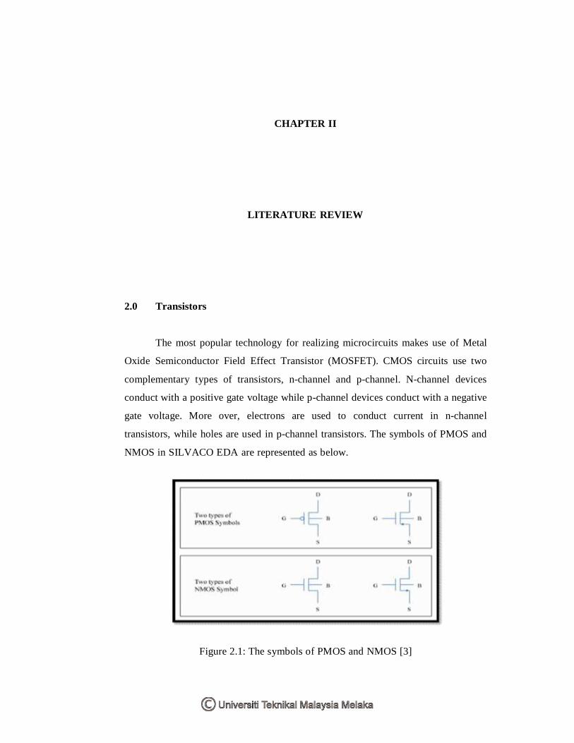
2.0 Transistors
The most popular technology for realizing microcircuits makes use of Metal
Oxide Semiconductor Field Effect Transistor (MOSFET). CMOS circuits use two
complementary types of transistors, n-channel and p-channel. N-channel devices
conduct with a positive gate voltage while p-channel devices conduct with a negative
gate voltage. More over, electrons are used to conduct current in n-channel
transistors, while holes are used in p-channel transistors. The symbols of PMOS and
NMOS in SILVACO EDA are represented as below.
Figure 2.1: The symbols of PMOS and NMOS [3]
6
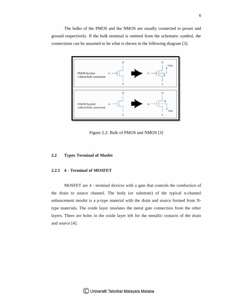
The bulks of the PMOS and the NMOS are usually connected to power and
ground respectively. If the bulk terminal is omitted from the schematic symbol, the
connections can be assumed to be what is shown in the following diagram [3].
Figure 2.2: Bulk of PMOS and NMOS [3]
2.2 Types Terminal of Mosfet
2.2.1 4 - Terminal of MOSFET
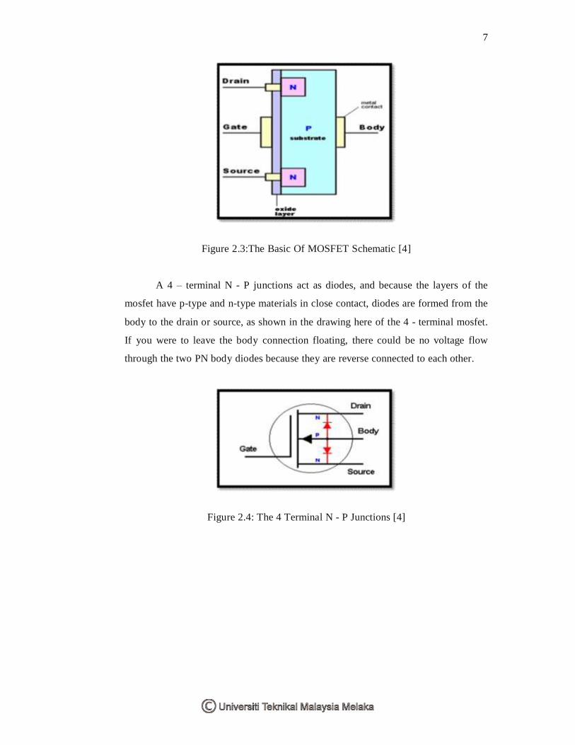
MOSFET are 4 - terminal devices with a gate that controls the conduction of
the drain to source channel. The body (or substrate) of the typical n-channel
enhancement mosfet is a p-type material with the drain and source formed from N-
type materials. The oxide layer insulates the metal gate connection from the other
layers. There are holes in the oxide layer left for the metallic contacts of the drain
and source [4].
7
Figure 2.3:The Basic Of MOSFET Schematic [4]
A 4 – terminal N - P junctions act as diodes, and because the layers of the
mosfet have p-type and n-type materials in close contact, diodes are formed from the
body to the drain or source, as shown in the drawing here of the 4 - terminal mosfet.
If you were to leave the body connection floating, there could be no voltage flow
through the two PN body diodes because they are reverse connected to each other.
Figure 2.4: The 4 Terminal N - P Junctions [4]
8
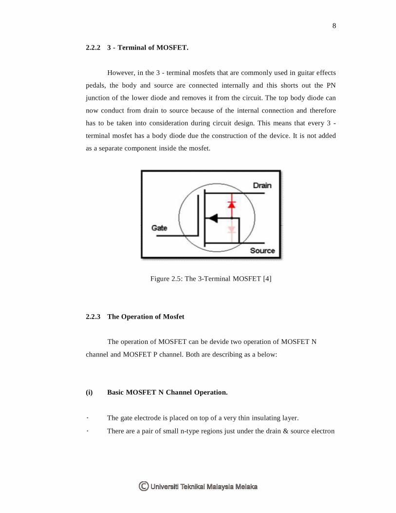
2.2.2 3 - Terminal of MOSFET.
However, in the 3 - terminal mosfets that are commonly used in guitar effects
pedals, the body and source are connected internally and this shorts out the PN
junction of the lower diode and removes it from the circuit. The top body diode can
now conduct from drain to source because of the internal connection and therefore
has to be taken into consideration during circuit design. This means that every 3 -
terminal mosfet has a body diode due the construction of the device. It is not added
as a separate component inside the mosfet.
Figure 2.5: The 3-Terminal MOSFET [4]
2.2.3 The Operation of Mosfet
The operation of MOSFET can be devide two operation of MOSFET N
channel and MOSFET P channel. Both are describing as a below:
(i) Basic MOSFET N Channel Operation.
· The gate electrode is placed on top of a very thin insulating layer.
· There are a pair of small n-type regions just under the drain & source electron