effects of rf power on structural properties of nc-si:h thin films
TRANSCRIPT
Sains Malaysiana 41(8)(2012): 993–1000
Effects of Rf Power on Structural Properties of Nc-Si:H Thin Films Deposited by Layer-By-Layer (LbL) Deposition Technique
(Kesan Kuasa Rf Terhadap Sifat-Sifat Struktur Filem Nipis Nc-Si:H yang dimendapkan dengan Menggunakan Teknik Lapisan Demi Lapisan (LbL)
GOH BOON TONG*, MUHAMAD RASAT MUHAMAD & SAADAH ABDUL RAHMAN
ABSTRAcT
The effects of rf power on the structural properties of hydrogenated nanocrystalline silicon (nc-Si:H) thin films deposited using layer-by-layer (LbL) deposition technique in a home-built plasma enhanced chemical vapor deposition (PECVD) system were investigated. The properties of the films were characterized by X-ray diffraction (XRD), micro-Raman scattering spectroscopy, high resolution transmission electron microscope (HRTEM) and Fourier transform infrared (FTIR) spectroscopy. The results showed that the films consisted of different size of Si crystallites embedded within an amorphous matrix and the growth of these crystallites was suppressed at higher rf powers. The crystalline volume fraction of the films was optimum at the rf power of 60 W and contained both small and big crystallites with diameters of 3.7 nm and 120 nm, respectively. The hydrogen content increased with increasing rf power and enhanced the structural disorder of the amorphous matrix thus decreasing the crystalline volume fraction of the films. Correlation of crystalline volume fraction, hydrogen content and structure disorder of the films under the effect of rf power is discussed.
Keywords: Crystalline volume fraction; hydrogen content; layer-by-layer deposition; ncSi:H; XRD
ABSTRAK
Dalam penyelidikan ini, kesan kuasa rf terhadap struktur filem nipis nanohablur silikon berhidrogen (nc-Si:H) yang dimendapkan menggunakan teknik lapisan demi lapisan (LbL) daripada sistem pemendapan wap kimia secara peningkatan plasma (PECVD) buatan sendiri telah dikaji. Sifat-sifat struktur filem nipis ini dikaji dengan kaedah belauan sinar-X (XRD), spektroskopi penyebaran mikro-Raman, mikroskopi elektron imbasan beresolusi tinggi (HRTEM) dan spektroskopi transformasi Fourier inframerah (FTIR). Keputusan menunjukkan bahawa filem nipis ini mengandungi hablur nano Si yang berlainan saiz yang terbenam dalam matriks amorfus. Pertumbuhan hablur nano Si ini terbantut pada kuasa rf yang lebih tinggi. Pecahan isi padu hablur filem nipis ini mencapai nilai optimum pada kuasa rf 60 W yang mengandungi kristalit silikon yang bersaiz kecil dan besar dengan diameter 3.7 and 120 nm. Kandungan hidrogen meningkat dengan menambahkan kuasa rf. Ini meningkatkan struktur tak tertib matriks amorfus dan pecahan isi padu hablur dalam filem nipis dapat dikurangkan. Korelasi di antara pecahan isi padu hablur, kandungan hidrogen dan struktur tak tertib filem nipis dengan kesan kuasa rf dibincangkan.
Kata kunci: Kandungan hydrogen; nc-Si:H; pemendapan LbL; XRD; pecahan isipadu hablur
INTRODUcTION
Hydrogenated nanocrystalline silicon (nc-Si:H) thin films have recently attracted remarkable attention due to their superior optoelectronic properties and better stability comparable to hydrogenated amorphous silicon (a-Si:H) films (Hatzopoulos et al. 2006; Raha & Das 2008; Swain & Hwang 2009; Wang et al. 2004; Yue et al. 2006). The presence of silicon nano-crystallites embedded within the amorphous matrix of the film structure modifies the hydrogen bonding configuration thus improves the structural order in the film (Ali 2006; Chen et al. 2006). When applied in solar cells, these films can enhance the conversion efficiency and reduce light soaking effects (Adhikary & Ray 2007).
This film is usually grown with continuous plasma enhanced chemical vapor deposition (PEcVD) using silane, which is highly diluted with hydrogen in order to enhance the crystallization during the hydrogen etching effect (Wang & Wu 2007). However, hydrogen etching effect reduces the growth rate of the material. Many studies have investigated the role of hydrogen in the properties of the material prepared by various methods, such as PEcVD (Itoh et al. 2000), hot-wire cVD (HWcVD) (Alpuim & chu 1999) and electron cyclotron resonance cVD (EcRcVD) (choi et al. 1997). Recently, the layer-by-layer (LbL) deposition technique has been reported to produce materials with high crystallinity for device applications, such as fast photo-detecting devices (Ambrosone et al. 2003; Cabarrocas
994
2004; Lin et al. 2006). In the LbL deposition technique, hydrogen plasma treatment has been reported as a way to simply control the incorporation of hydrogen into the materials by hydrogen etching (Goh et al. 2008a, 2008b, 2009). The films that were fabricated with the LbL technique were highly crystalline and showed the highest deposition rate relative to those fabricated in previous works. In this work, nc-Si:H thin films have been deposited by LbL deposition technique in a home-built PEcVD system at different rf powers. The structural properties of the films were characterized by X-ray diffraction (XRD), micro-Raman scattering spectroscopy, high resolution transmission electron microscope (HRTEM) and Fourier transform infrared (FTIR) spectroscopy. The objective of this work was to study the effects of rf power on the structural properties of the films deposited by LbL deposition technique. The correlation of crystalline volume fraction, hydrogen content and structure disorder of the films under the effect of rf power will also be discussed.
EXpeRIMenTAL DETAILS
nc-Si:H films were deposited with the LbL deposition technique using a home-built radio-frequency (13.56 MHz) PEcVD system on p-type crystal silicon (111) substrates with mixed silane (SiH4) and hydrogen (H2) gases, as detailed in our earlier publication (Goh & Rahman 2006). During the LbL deposition process, a continuous SiH4 and H2 plasma was obtained from constant flow-rates of SiH4 and H2 of 5 sccm and 100 sccm, respectively. The deposition pressure and temperature were maintained at 0.8 mbar and 300°c, respectively, throughout the deposition process. The rf power was varied from 20 W to 100 W with 20 W intervals. In the LbL processes, the deposition was performed by periodically alternating the deposition of nc-Si:H layers for five minutes and hydrogen treatment layers for three minutes. This process was repeated for four cycles of 32 min deposition each. This LbL mode can be accomplished by switching off the silane source at the end of each cycle of nc-Si:H layer deposition with a mass flow controller. A hydrogen plasma treatment was applied to the surface of the substrate for 10 min before the deposition. These deposition conditions were chosen in this work because they were found to produce high crystallinity in the deposited films. The X-ray diffraction measurement was carried out using a SIEMENS D5000 X-ray diffractometer with CuKα X-ray radiation (λ = 1.5418 Å). The spectra were taken at an incidence angle of 2°. The Raman scattering spectra of the films were recorded with a Horiba Jobin Yvon 800 UV micro-Raman Spectrometer with a ccD detector. An Ar+ laser with a wavelength of 514.5 nm and power of 20 mW was used as the excitation source and the laser was focused onto a spot of 1 µm in diameter to collect the backscattered light from the samples. The HRTEM micrograph was obtained with a TEM (JeOL JeM-2100F) operating at 200
kV. The silicon-hydrogen bonding configurations and microstructure parameter of the films were investigated by FTIR spectra in the range of 4000 cm-1 – 400 cm-1 (Perkin-elmer System 2000).
RESULTS AND DIScUSSION
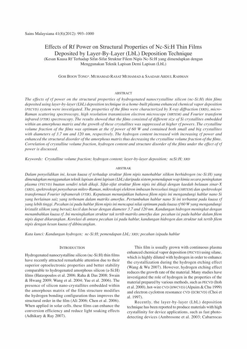
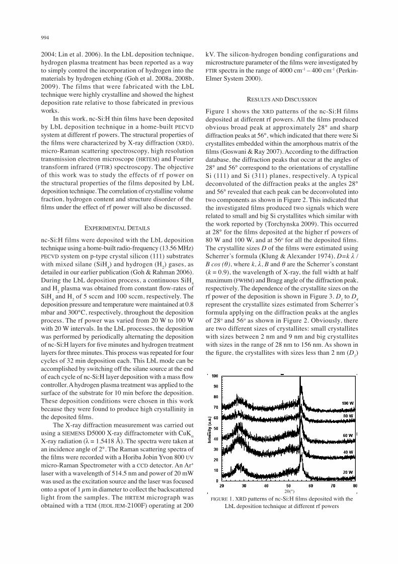
Figure 1 shows the XRD patterns of the nc-Si:H films deposited at different rf powers. All the films produced obvious broad peak at approximately 28° and sharp diffraction peaks at 56°, which indicated that there were Si crystallites embedded within the amorphous matrix of the films (Goswani & Ray 2007). According to the diffraction database, the diffraction peaks that occur at the angles of 28° and 56° correspond to the orientations of crystalline Si (111) and Si (311) planes, respectively. A typical deconvoluted of the diffraction peaks at the angles 28° and 56° revealed that each peak can be deconvoluted into two components as shown in Figure 2. This indicated that the investigated films produced two signals which were related to small and big Si crystallites which similar with the work reported by (Torchynska 2009). This occurred at 28° for the films deposited at the higher rf powers of 80 W and 100 W, and at 56o for all the deposited films. The crystallite sizes D of the films were estimated using Scherrer’s formula (Klung & Alexander 1974), D=k λ / B cos (θ), where k, λ, B and θ are the Scherrer’s constant (k = 0.9), the wavelength of X-ray, the full width at half maximum (FWHM) and Bragg angle of the diffraction peak, respectively. The dependence of the crystallite sizes on the rf power of the deposition is shown in Figure 3. D1 to D4 represent the crystallite sizes estimated from Scherrer’s formula applying on the diffraction peaks at the angles of 28o and 56o as shown in Figure 2. Obviously, there are two different sizes of crystallites: small crystallites with sizes between 2 nm and 9 nm and big crystallites with sizes in the range of 28 nm to 156 nm. As shown in the figure, the crystallites with sizes less than 2 nm (D1)
FIGURE 1. XRD patterns of nc-Si:H films deposited with the LbL deposition technique at different rf powers
2θ(°)
995
remain constant as the rf power is varied. The crystallite sizes (D4) remain constant at rf powers of 20 W to 60 W, increase to 8 nm with further increase in rf power to 80 W and remain constant at 100 W. The crystallite sizes (D2) show no change at higher rf powers. The crystallite sizes (D3) showed a decreasing trend as the rf power increase to 80 W and remain constant with further increase in rf power up to 100 W. This trend is the reverse of that encountered in conventional PEcVD, where the crystallite size increased with increasing rf power. Also, all the crystallites sizes remain constant at the higher rf powers of 80 W and 100 W, which is an interesting feature of the LbL deposition process. At low rf powers, the low dissociation rates of SiH4 and H2 in the deposition process and the low hydrogen etching rate contributed to the formation of small crystallite sizes in the films. At higher rf powers the ion bombardment effect on the growing surface increases, which enhances the effective surface temperature of the film and results in the increased crystallite size of the film (Hazra et al. 1999). However, in the LbL deposition process, an increase in rf power spontaneously increased the hydrogen etching in the hydrogen treatment process, which reduced the size of big crystallites but has no influence on the size of the small crystallites. Obviously, the big crystallites are grown
FIGURE 2. A typical deconvoluted of crystalline silicon peaks in XRD spectrum of the nc-Si:H film. The deconvoluted
components labeled as 1, 2, 3 and 4 represent the crystalline components correspond to the different crystallite sizes
FIGURE 3. Dependence of crystallite sizes versus rf power for the films deposited with the LBL deposition technique.
D1-4 represents the crystallite sizes estimated from Scherrer’s formula for the crystalline components labeled as
1 to 4, as shown in Figure 2
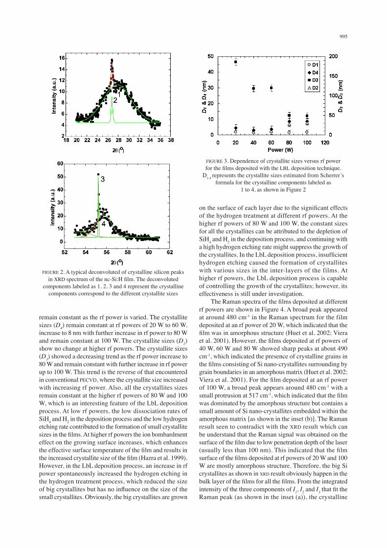
on the surface of each layer due to the significant effects of the hydrogen treatment at different rf powers. At the higher rf powers of 80 W and 100 W, the constant sizes for all the crystallites can be attributed to the depletion of SiH4 and H2 in the deposition process, and continuing with a high hydrogen etching rate might suppress the growth of the crystallites. In the LbL deposition process, insufficient hydrogen etching caused the formation of crystallites with various sizes in the inter-layers of the films. At higher rf powers, the LbL deposition process is capable of controlling the growth of the crystallites; however, its effectiveness is still under investigation. The Raman spectra of the films deposited at different rf powers are shown in Figure 4. A broad peak appeared at around 480 cm-1 in the Raman spectrum for the film deposited at an rf power of 20 W, which indicated that the film was in amorphous structure (Huet et al. 2002; Viera et al. 2001). However, the films deposited at rf powers of 40 W, 60 W and 80 W showed sharp peaks at about 490 cm-1, which indicated the presence of crystalline grains in the films consisting of Si nano-crystallites surrounding by grain boundaries in an amorphous matrix (Huet et al. 2002; Viera et al. 2001). For the film deposited at an rf power of 100 W, a broad peak appears around 480 cm-1 with a small protrusion at 517 cm-1, which indicated that the film was dominated by the amorphous structure but contains a small amount of Si nano-crystallites embedded within the amorphous matrix [as shown in the inset (b)]. The Raman result seen to contradict with the XRD result which can be understand that the Raman signal was obtained on the surface of the film due to low penetration depth of the laser (usually less than 100 nm). This indicated that the film surface of the films deposited at rf powers of 20 W and 100 W are mostly amorphous structure. Therefore, the big Si crystallites as shown in XRD result obviously happen in the bulk layer of the films for all the films. From the integrated intensity of the three components of I1, I2 and I3 that fit the Raman peak (as shown in the inset (a)), the crystalline
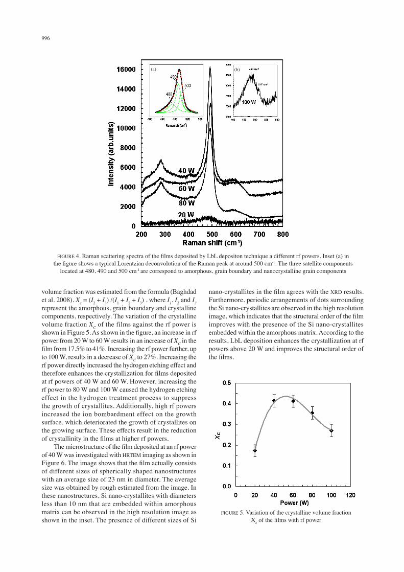
996
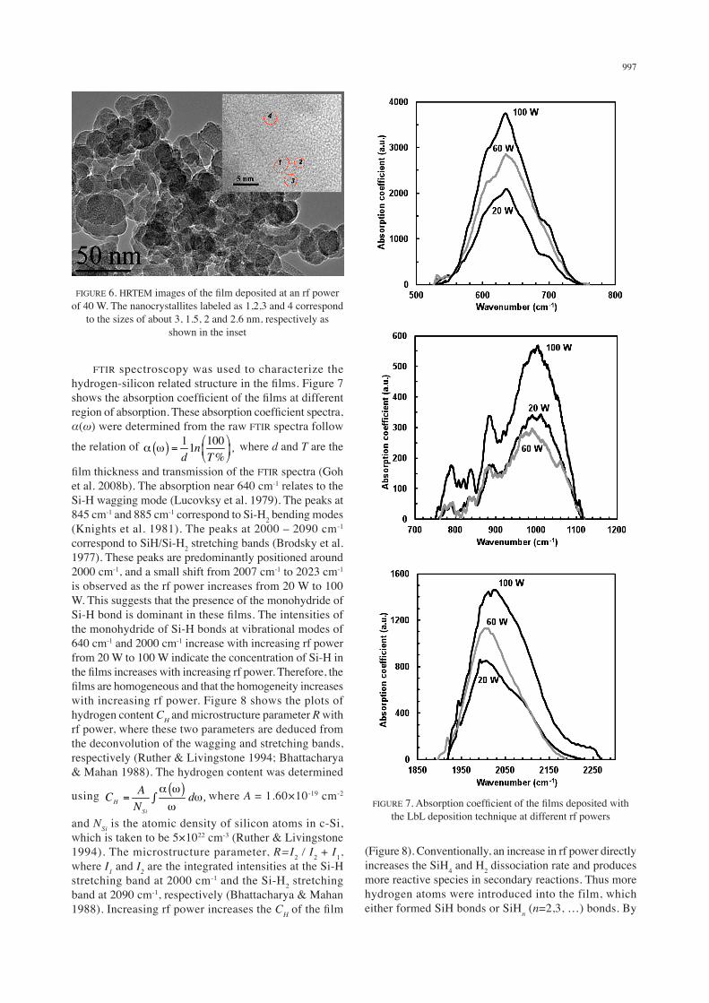
volume fraction was estimated from the formula (Baghdad et al. 2008), Xc = (I2 + I3) /(I1 + I2 + I3) , where I1, I2 and I3 represent the amorphous, grain boundary and crystalline components, respectively. The variation of the crystalline volume fraction XC of the films against the rf power is shown in Figure 5. As shown in the figure, an increase in rf power from 20 W to 60 W results in an increase of XC in the film from 17.5% to 41%. Increasing the rf power further, up to 100 W, results in a decrease of XC to 27%. Increasing the rf power directly increased the hydrogen etching effect and therefore enhances the crystallization for films deposited at rf powers of 40 W and 60 W. However, increasing the rf power to 80 W and 100 W caused the hydrogen etching effect in the hydrogen treatment process to suppress the growth of crystallites. Additionally, high rf powers increased the ion bombardment effect on the growth surface, which deteriorated the growth of crystallites on the growing surface. These effects result in the reduction of crystallinity in the films at higher rf powers. The microstructure of the film deposited at an rf power of 40 W was investigated with HRTEM imaging as shown in Figure 6. The image shows that the film actually consists of different sizes of spherically shaped nanostructures with an average size of 23 nm in diameter. The average size was obtained by rough estimated from the image. In these nanostructures, Si nano-crystallites with diameters less than 10 nm that are embedded within amorphous matrix can be observed in the high resolution image as shown in the inset. The presence of different sizes of Si
nano-crystallites in the film agrees with the XRD results. Furthermore, periodic arrangements of dots surrounding the Si nano-crystallites are observed in the high resolution image, which indicates that the structural order of the film improves with the presence of the Si nano-crystallites embedded within the amorphous matrix. According to the results, LbL deposition enhances the crystallization at rf powers above 20 W and improves the structural order of the films.
FIGURE 5. Variation of the crystalline volume fraction Xc of the films with rf power
FIGURE 4. Raman scattering spectra of the films deposited by LbL depositon technique a different rf powers. Inset (a) in the figure shows a typical Lorentzian deconvolution of the Raman peak at around 500 cm-1. The three satellite components
located at 480, 490 and 500 cm-1 are correspond to amorphous, grain boundary and nanocrystalline grain components
(a) (b)
997
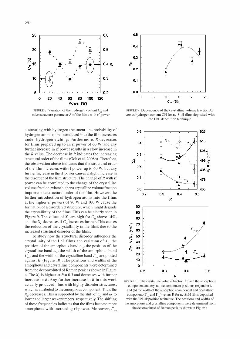
FTIR spectroscopy was used to characterize the hydrogen-silicon related structure in the films. Figure 7 shows the absorption coefficient of the films at different region of absorption. These absorption coefficient spectra, α(ω) were determined from the raw FTIR spectra follow
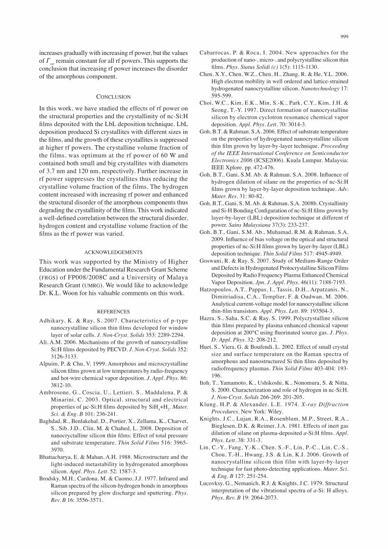
the relation of where d and T are the film thickness and transmission of the FTIR spectra (Goh et al. 2008b). The absorption near 640 cm-1 relates to the Si-H wagging mode (Lucovksy et al. 1979). The peaks at 845 cm-1 and 885 cm-1 correspond to Si-H2 bending modes (Knights et al. 1981). The peaks at 2000 – 2090 cm-1 correspond to SiH/Si-H2 stretching bands (Brodsky et al. 1977). These peaks are predominantly positioned around 2000 cm-1, and a small shift from 2007 cm-1 to 2023 cm-1 is observed as the rf power increases from 20 W to 100 W. This suggests that the presence of the monohydride of Si-H bond is dominant in these films. The intensities of the monohydride of Si-H bonds at vibrational modes of 640 cm-1 and 2000 cm-1 increase with increasing rf power from 20 W to 100 W indicate the concentration of Si-H in the films increases with increasing rf power. Therefore, the films are homogeneous and that the homogeneity increases with increasing rf power. Figure 8 shows the plots of hydrogen content CH and microstructure parameter R with rf power, where these two parameters are deduced from the deconvolution of the wagging and stretching bands, respectively (Ruther & Livingstone 1994; Bhattacharya & Mahan 1988). The hydrogen content was determined
using where A = 1.60×10⁻¹⁹ cm-2
and NSi is the atomic density of silicon atoms in c-Si, which is taken to be 5×1022 cm-3 (Ruther & Livingstone 1994). The microstructure parameter, R=I2 / I2 + I1, where I1 and I2 are the integrated intensities at the Si-H stretching band at 2000 cm-1 and the Si-H2 stretching band at 2090 cm-1, respectively (Bhattacharya & Mahan 1988). Increasing rf power increases the CH of the film
FIGURE 6. HRTEM images of the film deposited at an rf power of 40 W. The nanocrystallites labeled as 1,2,3 and 4 correspond
to the sizes of about 3, 1.5, 2 and 2.6 nm, respectively as shown in the inset
FIGURE 7. Absorption coefficient of the films deposited with the LbL deposition technique at different rf powers
(Figure 8). Conventionally, an increase in rf power directly increases the SiH4 and H2 dissociation rate and produces more reactive species in secondary reactions. Thus more hydrogen atoms were introduced into the film, which either formed SiH bonds or SiHn (n=2,3, …) bonds. By
998
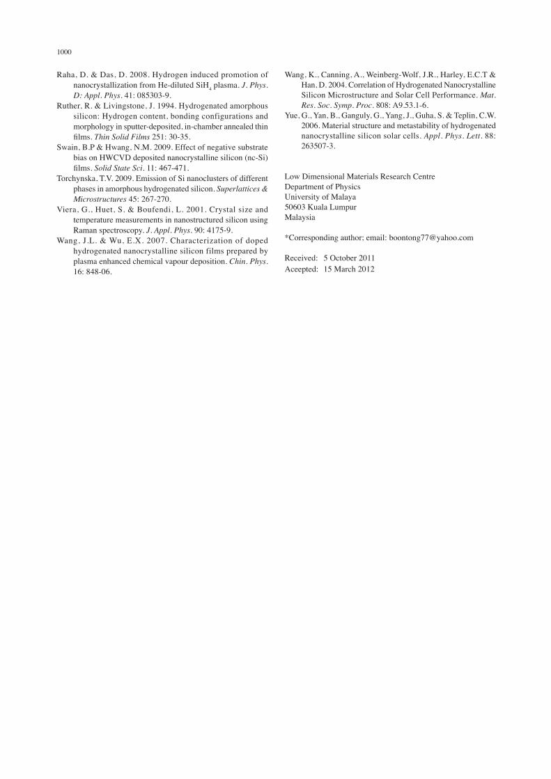
alternating with hydrogen treatment, the probability of hydrogen atoms to be introduced into the film increases under hydrogen etching. Furthermore, R decreases for films prepared up to an rf power of 60 W, and any further increase in rf power results in a slow increase in the R value. The decrease in R indicates the increasing structural order of the films (Goh et al. 2008b). Therefore, the observation above indicates that the structural order of the film increases with rf power up to 60 W, but any further increase in the rf power causes a slight increase in the disorder of the film structure. The change of R with rf power can be correlated to the change of the crystalline volume fraction, where higher a crystalline volume fraction improves the structural order of the film. However, the further introduction of hydrogen atoms into the films at the higher rf powers of 80 W and 100 W cause the formation of a disordered structure, which might degrade the crystallinity of the films. This can be clearly seen in Figure 9. The values of XC are high for CH above 14%, and the XC decreases if CH increases further. This causes the reduction of the crystallinity in the films due to the increased structural disorder of the films. To study how the structural disorder influences the crystallinity of the LbL films, the variation of XC, the position of the amorphous band ωa, the position of the crystalline band ωc, the width of the amorphous band Γωa, and the width of the crystalline band Γωc are plotted against R, (Figure 10). The positions and widths of the amorphous and crystalline components were determined from the deconvoluted of Raman peak as shown in Figure 4. The XC is highest at R = 0.3 and decreases with further increase in R. Any further increase in R in this work actually produced films with highly disorder structures, which is attributed to the amorphous component. Thus, the XC decreases. This is supported by the shift of ωa and ωc to lower and larger wavenumbers, respectively. The shifting of these frequencies indicates that the films become more amorphous with increasing rf power. Moreover, Γωa
FIGURE 8. Variation of the hydrogen content CH and microstructure parameter R of the films with rf power
FIGURE 9. Dependence of the crystalline volume fraction Xc versus hydrogen content CH for nc-Si:H films deposited with
the LbL deposition technique
FIGURE 10. The crystalline volume fraction Xc and the amorphous component and crystalline component positions (ωa and ωc),
and (b) the width of the amorphous component and crystalline component (Γωa and Γωc) versus R for nc-Si:H films deposited with the LbL deposition technique. The positions and widths of
the amorphous and crystalline components were determined from the deconvoluted of Raman peak as shown in Figure 4
999
increases gradually with increasing rf power, but the values of Γωc remain constant for all rf powers. This supports the conclusion that increasing rf power increases the disorder of the amorphous component.
cONcLUSION
In this work, we have studied the effects of rf power on the structural properties and the crystallinity of nc-Si:H films deposited with the LbL deposition technique. LbL deposition produced Si crystallites with different sizes in the films, and the growth of these crystallites is suppressed at higher rf powers. The crystalline volume fraction of the films, was optimum at the rf power of 60 W and contained both small and big crystallites with diameters of 3.7 nm and 120 nm, respectively. Further increase in rf power suppresses the crystallites thus reducing the crystalline volume fraction of the films. The hydrogen content increased with increasing rf power and enhanced the structural disorder of the amorphous components thus degrading the crystallinity of the films. This work indicated a well-defined correlation between the structural disorder, hydrogen content and crystalline volume fraction of the films as the rf power was varied.
AcKNOWLEDGEMENTS
This work was supported by the Ministry of Higher Education under the Fundamental Research Grant Scheme (FRGS) of FP008/2008c and a University of Malaya Research Grant (UMRG). We would like to acknowledge Dr. K.L. Woon for his valuable comments on this work.
REFERENcES
Adhikary, K. & Ray, S. 2007. Characteristics of p-type nanocrystalline silicon thin films developed for window layer of solar cells. J. Non-Cryst. Solids 353: 2289-2294.
Ali, A.M. 2006. Mechanisms of the growth of nanocrystalline Si:H films deposited by peCVD. J. Non-Cryst. Solids 352: 3126-3133.
Alpuim, p. & Chu, V. 1999. Amorphous and microcrystalline silicon films grown at low temperatures by radio-frequency and hot-wire chemical vapor deposition. J. Appl. Phys. 86: 3812-10.
Ambrosone, G., Coscia, U., Lettieri, S., Maddalena, p. & Minarini, C. 2003. Optical, structural and electrical properties of μc-Si:H films deposited by SiH4+H2. Mater. Sci. & Eng. B 101: 236-241.
Baghdad, R., Benlakehal, D., portier, X., Zellama, K., Charvet, S., Sib, J.D., Clin, M. & Chahed, L. 2008. Deposition of nanocryctalline silicon thin films: effect of total pressure and substrate temperature. Thin Solid Films 516: 3965-3970.
Bhattacharya, e. & Mahan, A.H. 1988. Microstructure and the light-induced metastability in hydrogenated amorphous silicon. Appl. Phys. Lett. 52: 1587-3.
Brodsky, M.H., Cardona, M. & Cuomo, J.J. 1977. Infrared and Raman spectra of the silicon-hydrogen bonds in amorphous silicon prepared by glow discharge and sputtering. Phys. Rev. B 16: 3556-3571.
Cabarrocas, p. & Roca, I. 2004. new approaches for the production of nano-, micro-, and polycrystalline silicon thin films. Phys. Status Solidi (c) 1(5): 1115-1130.
Chen, X.Y., Chen, W.Z., Chen, H., Zhang, R. & He, Y.L. 2006. High electron mobility in well ordered and lattice-strained hydrogenated nanocrystalline silicon. Nanotechnology 17: 595-599.
Choi, W.C., Kim, e.K., Min, S.-K., park, C.Y., Kim, J.H. & Seong, T.-Y. 1997. Direct formation of nanocrystalline silicon by electron cyclotron resonance chemical vapor deposition. Appl. Phys. Lett. 70: 3014-3.
Goh, B.T. & Rahman, S.A. 2006. effect of substrate temperature on the properties of hydrogenated nanocrystalline silicon thin film grown by layer-by-layer technique. Proceeding of the IEEE International Conference on Semiconductor Electronics 2006 (ICSe2006). Kuala Lumpur. Malaysia: Ieee Xplore. pp. 472-476.
Goh, B.T., Gani, S.M. Ab. & Rahman, S.A. 2008. Influence of hydrogen dilution of silane on the properties of nc-Si:H films grown by layer-by-layer deposition technique. Adv. Mater. Res. 31: 80-82.
Goh, B.T., Gani, S. M. Ab. & Rahman, S.A. 2008b. Crystallinity and Si-H Bonding Configuration of nc-Si:H films grown by layer-by-layer (LBL) deposition technique at different rf power. Sains Malaysiana 37(3): 233-237.
Goh, B.T., Gani, S.M. Ab., Muhamad, R.M. & Rahman, S.A. 2009. Influence of bias voltage on the optical and structural properties of nc-Si:H films grown by layer-by-layer (LBL) deposition technique. Thin Solid Films 517: 4945-4949.
Goswani, R. & Ray, S. 2007. Study of Medium-Range Order and Defects in Hydrogenated Protocrystalline Silicon Films Deposited by Radio Frequency Plasma Enhanced chemical Vapor Deposition. Jpn. J. Appl. Phys. 46(11): 7188-7193.
Hatzopoulos, A.T., pappas, I., Tassis, D.H., Arpatzanis, n., Dimitriadisa, C.A., Templier, F. & Oudwan, M. 2006. Analytical current-voltage model for nanocrystalline silicon thin-film transistors. Appl. Phys. Lett. 89: 193504-3.
Hazra, S., Saha, S.C. & Ray, S. 1999. polycrystalline silicon thin films prepared by plasma enhanced chemical vapour deposition at 200°C using fluorinated source gas. J. Phys. D: Appl. Phys. 32: 208-212.
Huet, S., Viera, G. & Boufendi, L. 2002. effect of small crystal size and surface temperature on the Raman spectra of amorphous and nanostructured Si thin films deposited by radiofrequency plasmas. Thin Solid Films 403-404: 193-196.
Itoh, T., Yamamoto, K., Ushikoshi, K., nonomura, S. & nitta, S. 2000. Characterization and role of hydrogen in nc-Si:H. J. Non-Cryst. Solids 266-269: 201-205.
Klung, H.p. & Alexander, L.e. 1974. X-ray Diffraction Procedures. new York: Wiley.
Knights, J.C., Lujan, R.A., Rosenblum, M.p., Street, R.A., Bieglesen, D.K. & Reimer, J.A. 1981. effects of inert gas dilution of silane on plasma-deposited a-Si:H films. Appl. Phys. Lett. 38: 331-3.
Lin, C.-Y., Fang, Y.-K., Chen, S.-F., Lin, p.-C., Lin, C.-S., Chou, T.-H., Hwang, J.S. & Lin, K.I. 2006. Growth of nanocrystalline silicon thin film with layer-by-layer technique for fast photo-detecting applications. Mater. Sci. & Eng. B 127: 251-254.
Lucovksy, G., nemanich, R.J. & Knights, J.C. 1979. Structural interpretation of the vibrational spectra of a-Si: H alloys. Phys. Rev. B 19: 2064-2073.
1000
Raha, D. & Das, D. 2008. Hydrogen induced promotion of nanocrystallization from He-diluted SiH4 plasma. J. Phys. D: Appl. Phys. 41: 085303-9.
Ruther, R. & Livingstone, J. 1994. Hydrogenated amorphous silicon: Hydrogen content, bonding configurations and morphology in sputter-deposited, in-chamber annealed thin films. Thin Solid Films 251: 30-35.
Swain, B.p & Hwang, n.M. 2009. effect of negative substrate bias on HWcVD deposited nanocrystalline silicon (nc-Si) films. Solid State Sci. 11: 467-471.
Torchynska, T.V. 2009. emission of Si nanoclusters of different phases in amorphous hydrogenated silicon. Superlattices & Microstructures 45: 267-270.
Viera, G., Huet, S. & Boufendi, L. 2001. Crystal size and temperature measurements in nanostructured silicon using Raman spectroscopy. J. Appl. Phys. 90: 4175-9.
Wang, J.L. & Wu, e.X. 2007. Characterization of doped hydrogenated nanocrystalline silicon films prepared by plasma enhanced chemical vapour deposition. Chin. Phys. 16: 848-06.
Wang, K., Canning, A., Weinberg-Wolf, J.R., Harley, e.C.T & Han, D. 2004. correlation of Hydrogenated Nanocrystalline Silicon Microstructure and Solar cell performance. Mat. Res. Soc. Symp. Proc. 808: A9.53.1-6.
Yue, G., Yan, B., Ganguly, G., Yang, J., Guha, S. & Teplin, C.W. 2006. Material structure and metastability of hydrogenated nanocrystalline silicon solar cells. Appl. Phys. Lett. 88: 263507-3.
Low Dimensional Materials Research centreDepartment of PhysicsUniversity of Malaya50603 Kuala LumpurMalaysia
*Corresponding author; email: [email protected]
Received: 5 October 2011Aceepted: 15 March 2012