graphene growth at low temperatures using rf-plasma ... aishah khalid.pdf · graphene growth at low...
TRANSCRIPT
Sains Malaysiana 46(7)(2017): 1111–1117 http://dx.doi.org/10.17576/jsm-2017-4607-14
Graphene Growth at Low Temperatures using RF-Plasma Enhanced Chemical Vapour Deposition
(Pertumbuhan Grafin pada Suhu Rendah menggunakan Pemendapan Wap Kimia secara Peningkatan RF-Plasma)
AISHAH KHALID, MOHD AMBRI MOHAMED* & AKRAJAS ALI UMAR
ABSTRACT
The advantage of plasma enhanced chemical vapour deposition (PECVD) method is the ability to deposit thin films at relatively low temperature. Plasma power supports the growth process by decomposing hydrocarbon to carbon radicals which will be deposited later on metal catalyst. In this work, we have successfully synthesis graphene on Ni and Co films at relatively low temperature and optimize the synthesis conditions by adjusting the plasma power. Low temperature growth of graphene was optimized at 600°C after comparing the quality of as-grown graphene at several temperatures from 400 to 800°C and by varying plasma powers in the range of 20 - 100 W. Raman analysis of the as-grown samples showed that graphene prefers lower plasma power of 40 W. The annihilation of graphene formation at higher plasma powers is attributed to the presence of high concentration of hydrogen radical from methane which recombines with carbon elements on thin film surface. The optimum graphene growth conditions were obtained at growth temperature of 600°C, plasma power of 40 W and growth time of 10 min with methane flow rate of 120 sccm.
Keywords: Graphene growth; low temperature; PECVD; plasma
ABSTRAK
Kelebihan kaedah pemendapan wap kimia secara peningkatan plasma (PECVD) adalah keupayaan untuk endapan filem nipis pada suhu yang rendah. Kuasa plasma menyokong proses pertumbuhan dengan menguraikan hidrokarbon kepada unsur karbon aktif dan kemudian diserap oleh logam pemangkin. Dalam kajian ini, kami telah berjaya mensintesis grafin di atas filem Ni and Co pada suhu rendah dan mengoptimumkan keadaan sintesis dengan mengubah kuasa plasma. Suhu pertumbuhan rendah diperoleh pada 600°C setelah membandingkan kualiti grafin yang terhasil pada beberapa suhu lain daripada 400 kepada 800°C dengan mengubah kuasa plasma dalam lingkungan 20-100 W. Analisis Raman menunjukkan bahawa pertumbuhan grafin memerlukan kuasa plasma yang rendah iaitu 40 W. Penghapusan pembentukan grafin pada kuasa plasma yang lebih tinggi adalah disebabkan oleh kehadiran unsur aktif hidrogen yang berkepekatan tinggi daripada metana yang bergabung dengan unsur karbon pada permukaan filem nipis. Keadaan pertumbuhan grafin yang optimum diperoleh pada suhu pertumbuhan 600°C, kuasa plasma 40 W dan masa pertumbuhan 10 min dengan kadar aliran metana 120 sccm.
Kata kunci: Pertumbuhan grafin; PECVD; plasma; suhu rendah
INTRODUCTION
Graphene is one of the 2D materials in carbon allotropes family. Graphene has been given a great attention as the next generation material because of the excellent electrical, mechanical and optical characteristics. It can be regarded as one of the most promising materials for high-performance and flexible electronic devices such as thin-film transistors (Novoselov et al. 2004) super capacitor (El-Kady & Kaner 2013) and photodetector (Koybasi et al. 2012). To date there are various methods of graphene production (Choi & Lee 2012) such as mechanical exfoliation (Geim & Novoselov 2007), chemical synthesis (Kuila et al. 2012), graphene oxide (Noorhafanita et al. 2014), epitaxial growth (Juang et al. 2009) and chemical vapour deposition (CVD) growth (Shaharin Fadzli et al. 2014). All these methods have their advantages and disadvantages depending on the applications.
For large-area, uniform and high quality of graphene production, CVD method is preferred by the industry. There are many researches on growing graphene by using CVD onto the transition metal such Cu, Ni, Co and Pt. All these metals have different carbon solubility which is important in graphene formation. Cu has been categorized as low in carbon solubility compared to Ni and Co. Thus, many researchers had employed Cu foil as the metal substrate to produce single layer graphene (SLG) (Jin et al. 2014) compared to Ni and Co as their tendency to form multilayer graphene (Kim et al. 2011). However, one could reduce the graphene layers by reducing the thickness of Co films, as reported by Ramón et al. (2011). Normally, conventional CVD methods require a high temperature growth condition which is above 1000°C. This high temperature limits the choice of substrate as not all substrate can withstand the high temperatures. In this case,
1112
adding plasma to the CVD system helps to lower the growth temperature on the desired substrate with the support of metal catalyst. To date, many researchers demonstrate that PECVD is the promising alternative for lowering the graphene growth temperature. For example, Wang et al. (2013) reported the growth of few layers graphene on polycrystalline Co film at 800°C and study the effect of time growth toward the graphene crystallinity. Wang et al. (2010) also employed PECVD to grow graphene on Co film at low temperature (800°C) for 40 s using mix gas CH4/H2/Ar. Optimizing the growth conditions is crucial because some parameters need to be considered on this PECVD process such as growth temperature, growth time, plasma power and gas flow rate. By considering the plasma effect towards graphene formation, the growth condition for our PECVD system has been optimized. Methane (CH4) gas was used as hydrocarbon source, meanwhile Ni and Co films were used as the metal catalysts for growing graphene at relatively low temperatures with different plasma power. We also determined that the amount of plasma power has significant effect to the graphene formation. The optimum graphene growth conditions were obtained at growth temperature of 600°C, plasma power of 40 W and growth time of 10 min with methane flow rate of 120 sccm. It is expected that by fine tuning the other growth conditions such as cooling sequence and post-treatment of catalyst film, the synthesis temperature can be lowered further down to 200°C enabling the direct formation of graphene on a wide range of substrates including on PET and others
flexible substrates without complicated post-transfer processes.
MATERIALS AND METHODS
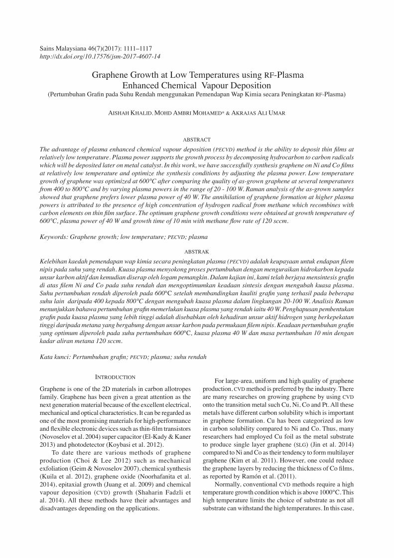
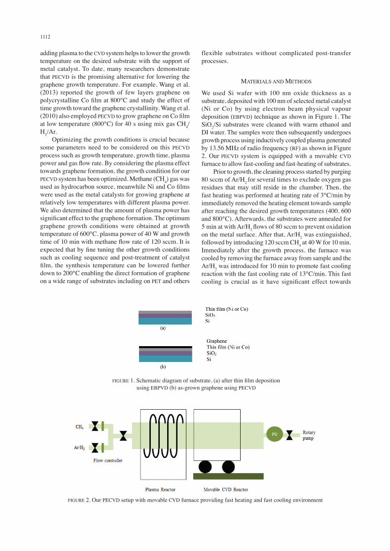
We used Si wafer with 100 nm oxide thickness as a substrate, deposited with 100 nm of selected metal catalyst (Ni or Co) by using electron beam physical vapour deposition (EBPVD) technique as shown in Figure 1. The SiO2/Si substrates were cleaned with warm ethanol and DI water. The samples were then subsequently undergoes growth process using inductively coupled plasma generated by 13.56 MHz of radio frequency (RF) as shown in Figure 2. Our PECVD system is equipped with a movable CVD furnace to allow fast-cooling and fast-heating of substrates. Prior to growth, the cleaning process started by purging 80 sccm of Ar/H2 for several times to exclude oxygen gas residues that may still reside in the chamber. Then, the fast heating was performed at heating rate of 3°C/min by immediately removed the heating element towards sample after reaching the desired growth temperatures (400, 600 and 800°C). Afterwards, the substrates were annealed for 5 min at with Ar/H2 flows of 80 sccm to prevent oxidation on the metal surface. After that, Ar/H2 was extinguished, followed by introducing 120 sccm CH4 at 40 W for 10 min. Immediately after the growth process, the furnace was cooled by removing the furnace away from sample and the Ar/H2 was introduced for 10 min to promote fast cooling reaction with the fast cooling rate of 13°C/min. This fast cooling is crucial as it have significant effect towards
FIGURE 1. Schematic diagram of substrate, (a) after thin film deposition using EBPVD (b) as-grown graphene using PECVD
FIGURE 2. Our PECVD setup with movable CVD furnace providing fast heating and fast cooling environment
1113
graphene formation (Dathbun & Chaisitsak 2013). The same steps were implemented to observe plasma effect at low temperatures by introducing different plasma powers (40, 80 and 100 W), while maintaining the growth time and CH4 flow rate at 10 min and 120 sccm, respectively. Finally, we characterized the as grown-graphene by using Raman spectroscopy, field emission scanning electron microscopy (FESEM) and x-ray photoelectron spectroscopy (XPS). Raman UNIRAM with an excitation wavelength of 532 nm under ambient condition was used to characterize graphene. Random spots are taken across all samples to estimate the quality and uniformity of the synthesized graphene. From Raman analysis, the appearance of graphene are observed by the rises of D, G and 2D peak at ~1300 cm-1, ~ 1580 cm-1 and 2700 cm-1, respectively. The D, G and 2D peak in Raman spectra refer to the defect on the graphene structure, sp2 vibration and stacking in graphene, respectively. The qualities of the as-grown graphene were further analyzed by XPS through the chemical bonding and FESEM was used to observed graphene morphology and grain size distribution.
RESULTS AND DISCUSSION
TEMPERATURE DEPENDENCE
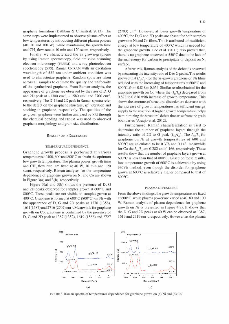
Graphene growth process is performed at various temperatures of 400, 600 and 800°C to obtain the optimum low growth temperature. The plasma power, growth time and CH4 flow rate, are fixed at 40 W, 10 min and 120 sccm, respectively. Raman analyses for the temperature dependence of graphene grown on Ni and Co are shown in Figure 3(a) and 3(b), respectively. Figure 3(a) and 3(b) shows the presence of D, G and 2D peaks observed for samples grown at 600°C and 800°C. Those peaks are not visible on samples grown at 400°C. Graphene is formed at 600°C (800°C) on Ni with the appearance of D, G and 2D peaks at 1370 (1358), 1611(1587) and 2716 (2702) cm-1. Meanwhile for graphene growth on Co, graphene is confirmed by the presence of D, G and 2D peak at 1387 (1352), 1619 (1586) and 2727
(2703) cm-1. However, at lower growth temperature of 400°C, the D, G and 2D peaks are absent for both samples grown on Ni and Co films. This is attributed to insufficient energy at low temperature of 400°C which is needed for the graphene growth. Lee et al. (2011) also proved that, there is no graphene observed at 550°C due to the lack of thermal energy for carbon to precipitate or deposit on Ni surface. Afterwards, Raman analysis of the defect is observed by measuring the intensity ratio of D to G peaks. The results showed that (ID/IG) for the as-grown graphene on Ni films reduced with the increasing of temperatures at 600°C and 800°C, from 0.818 to 0.654. Similar results obtained for the graphene growth on Co where the (ID/IG) decreased from 0.878 to 0.636 with increase of growth temperature. This shows the amounts of structural disorder are decrease with the increase of growth temperatures, as sufficient energy supply to the reaction at higher growth temperature, helps in minimizing the structural defect that arise from the grain boundaries (Araujo et al. 2012). Furthermore, Raman characterization is used to determine the number of graphene layers through the intensity ratio of 2D to G peak (I2D/IG). The I2D/IG for graphene on Ni at growth temperatures of 600 and 800°C are calculated to be 0.378 and 0.143, meanwhile for Co the I2D/IG are 0.282 and 0.166, respectively. These results show that the number of graphene layers grown at 600°C is less than that of 800°C. Based on these results, low temperature growth of 600°C is achievable by using PECVD method, even though the disorder for graphene grown at 600°C is relatively higher compared to that of 800°C.
PLASMA DEPENDENCE
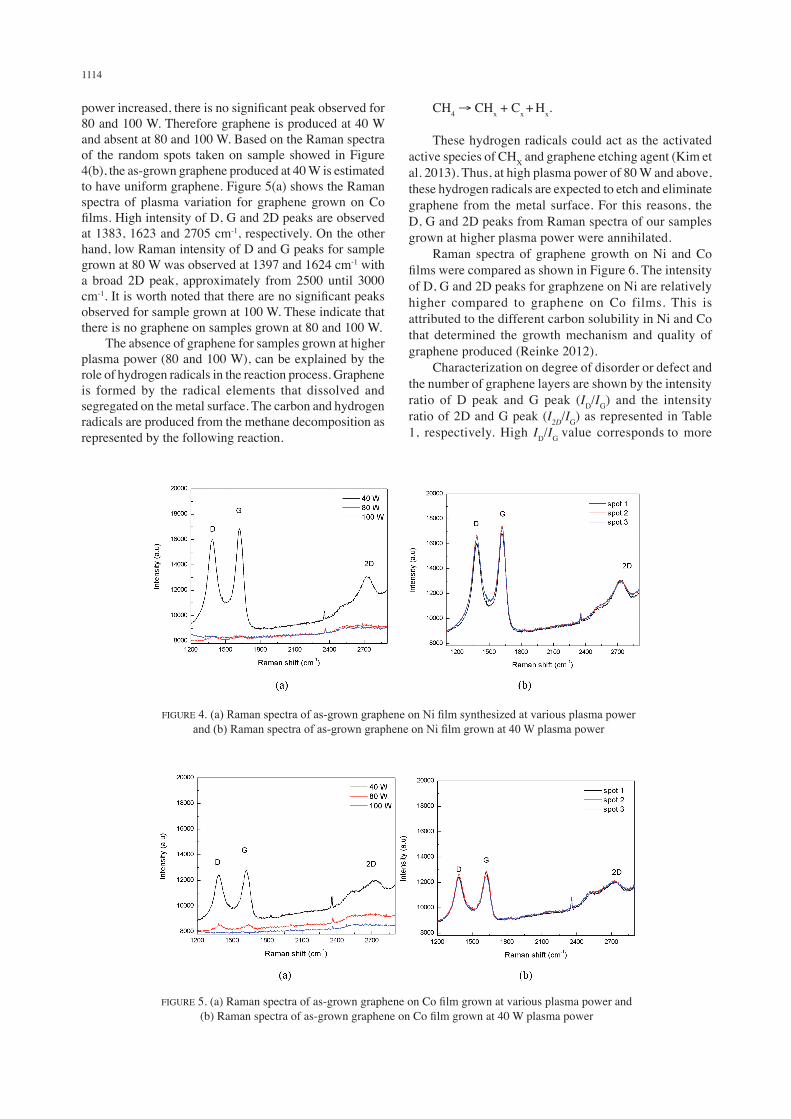
From the above findings, the growth temperature are fixed at 600°C, while plasma power are varied at 40, 80 and 100 W. Raman analysis of plasma dependence for graphene growth on Ni is presented in Figure 4(a). It shows that the D, G and 2D peaks at 40 W can be observed at 1387, 1619 and 2719 cm-1, respectively. However, as the plasma
FIGURE 3. Raman spectra of temperatures dependence for graphene grown on (a) Ni and (b) Co
1114
power increased, there is no significant peak observed for 80 and 100 W. Therefore graphene is produced at 40 W and absent at 80 and 100 W. Based on the Raman spectra of the random spots taken on sample showed in Figure 4(b), the as-grown graphene produced at 40 W is estimated to have uniform graphene. Figure 5(a) shows the Raman spectra of plasma variation for graphene grown on Co films. High intensity of D, G and 2D peaks are observed at 1383, 1623 and 2705 cm-1, respectively. On the other hand, low Raman intensity of D and G peaks for sample grown at 80 W was observed at 1397 and 1624 cm-1 with a broad 2D peak, approximately from 2500 until 3000 cm-1. It is worth noted that there are no significant peaks observed for sample grown at 100 W. These indicate that there is no graphene on samples grown at 80 and 100 W. The absence of graphene for samples grown at higher plasma power (80 and 100 W), can be explained by the role of hydrogen radicals in the reaction process. Graphene is formed by the radical elements that dissolved and segregated on the metal surface. The carbon and hydrogen radicals are produced from the methane decomposition as represented by the following reaction.
CH4 → CHx + Cx + Hx.
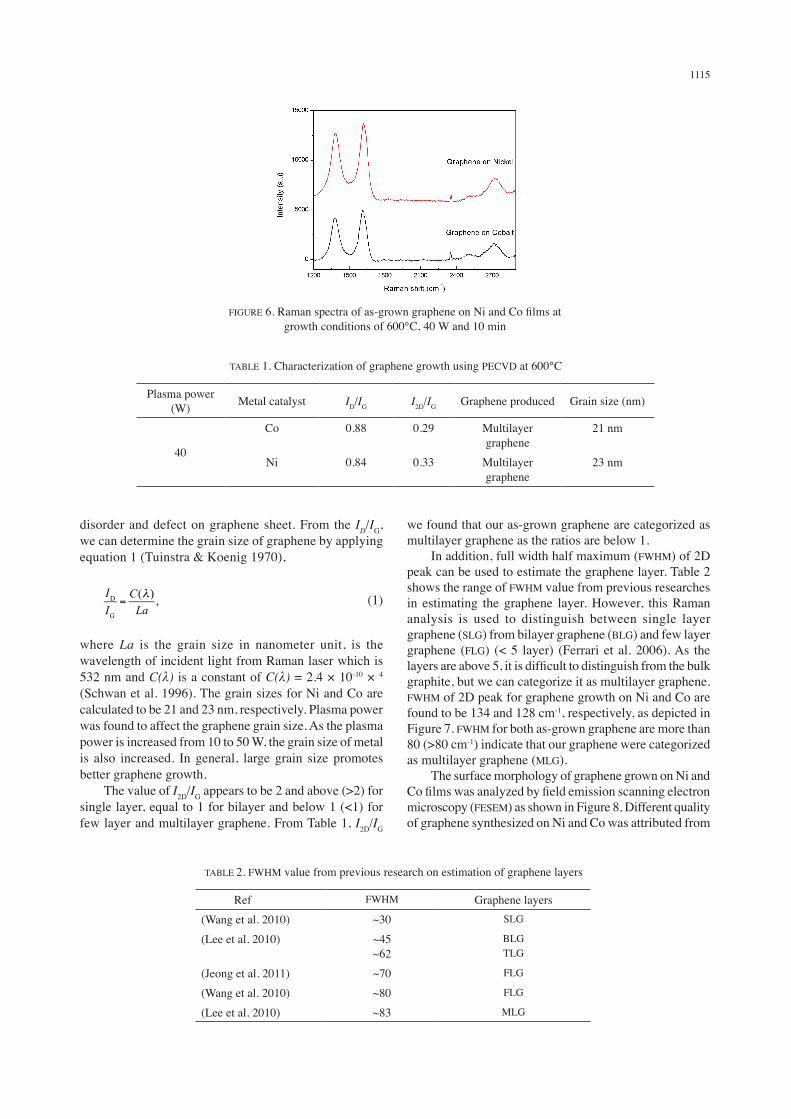
These hydrogen radicals could act as the activated active species of CHX and graphene etching agent (Kim et al. 2013). Thus, at high plasma power of 80 W and above, these hydrogen radicals are expected to etch and eliminate graphene from the metal surface. For this reasons, the D, G and 2D peaks from Raman spectra of our samples grown at higher plasma power were annihilated. Raman spectra of graphene growth on Ni and Co films were compared as shown in Figure 6. The intensity of D, G and 2D peaks for graphzene on Ni are relatively higher compared to graphene on Co films. This is attributed to the different carbon solubility in Ni and Co that determined the growth mechanism and quality of graphene produced (Reinke 2012). Characterization on degree of disorder or defect and the number of graphene layers are shown by the intensity ratio of D peak and G peak (ID/IG) and the intensity ratio of 2D and G peak (I2D/IG) as represented in Table 1, respectively. High ID/IG value corresponds to more
FIGURE 5. (a) Raman spectra of as-grown graphene on Co film grown at various plasma power and (b) Raman spectra of as-grown graphene on Co film grown at 40 W plasma power
FIGURE 4. (a) Raman spectra of as-grown graphene on Ni film synthesized at various plasma power and (b) Raman spectra of as-grown graphene on Ni film grown at 40 W plasma power
1115
disorder and defect on graphene sheet. From the ID/IG, we can determine the grain size of graphene by applying equation 1 (Tuinstra & Koenig 1970),
(1)
where La is the grain size in nanometer unit, is the wavelength of incident light from Raman laser which is 532 nm and C(λ) is a constant of C(λ) = 2.4 × 10-10 × 4
(Schwan et al. 1996). The grain sizes for Ni and Co are calculated to be 21 and 23 nm, respectively. Plasma power was found to affect the graphene grain size. As the plasma power is increased from 10 to 50 W, the grain size of metal is also increased. In general, large grain size promotes better graphene growth. The value of I2D/IG appears to be 2 and above (>2) for single layer, equal to 1 for bilayer and below 1 (<1) for few layer and multilayer graphene. From Table 1, I2D/IG
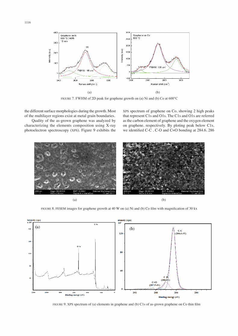
we found that our as-grown graphene are categorized as multilayer graphene as the ratios are below 1. In addition, full width half maximum (FWHM) of 2D peak can be used to estimate the graphene layer. Table 2 shows the range of FWHM value from previous researches in estimating the graphene layer. However, this Raman analysis is used to distinguish between single layer graphene (SLG) from bilayer graphene (BLG) and few layer graphene (FLG) (< 5 layer) (Ferrari et al. 2006). As the layers are above 5, it is difficult to distinguish from the bulk graphite, but we can categorize it as multilayer graphene. FWHM of 2D peak for graphene growth on Ni and Co are found to be 134 and 128 cm-1, respectively, as depicted in Figure 7. FWHM for both as-grown graphene are more than 80 (>80 cm-1) indicate that our graphene were categorized as multilayer graphene (MLG). The surface morphology of graphene grown on Ni and Co films was analyzed by field emission scanning electron microscopy (FESEM) as shown in Figure 8. Different quality of graphene synthesized on Ni and Co was attributed from
FIGURE 6. Raman spectra of as-grown graphene on Ni and Co films at growth conditions of 600°C, 40 W and 10 min
TABLE 1. Characterization of graphene growth using PECVD at 600°C
Plasma power (W) Metal catalyst ID/IG I2D/IG Graphene produced Grain size (nm)
40
Co 0.88 0.29 Multilayer graphene
21 nm
Ni 0.84 0.33 Multilayer graphene
23 nm
TABLE 2. FWHM value from previous research on estimation of graphene layers
Ref FWHM Graphene layers(Wang et al. 2010) ~30 SLG
(Lee et al. 2010) ~45~62
BLGTLG
(Jeong et al. 2011) ~70 FLG
(Wang et al. 2010) ~80 FLG
(Lee et al. 2010) ~83 MLG
1116
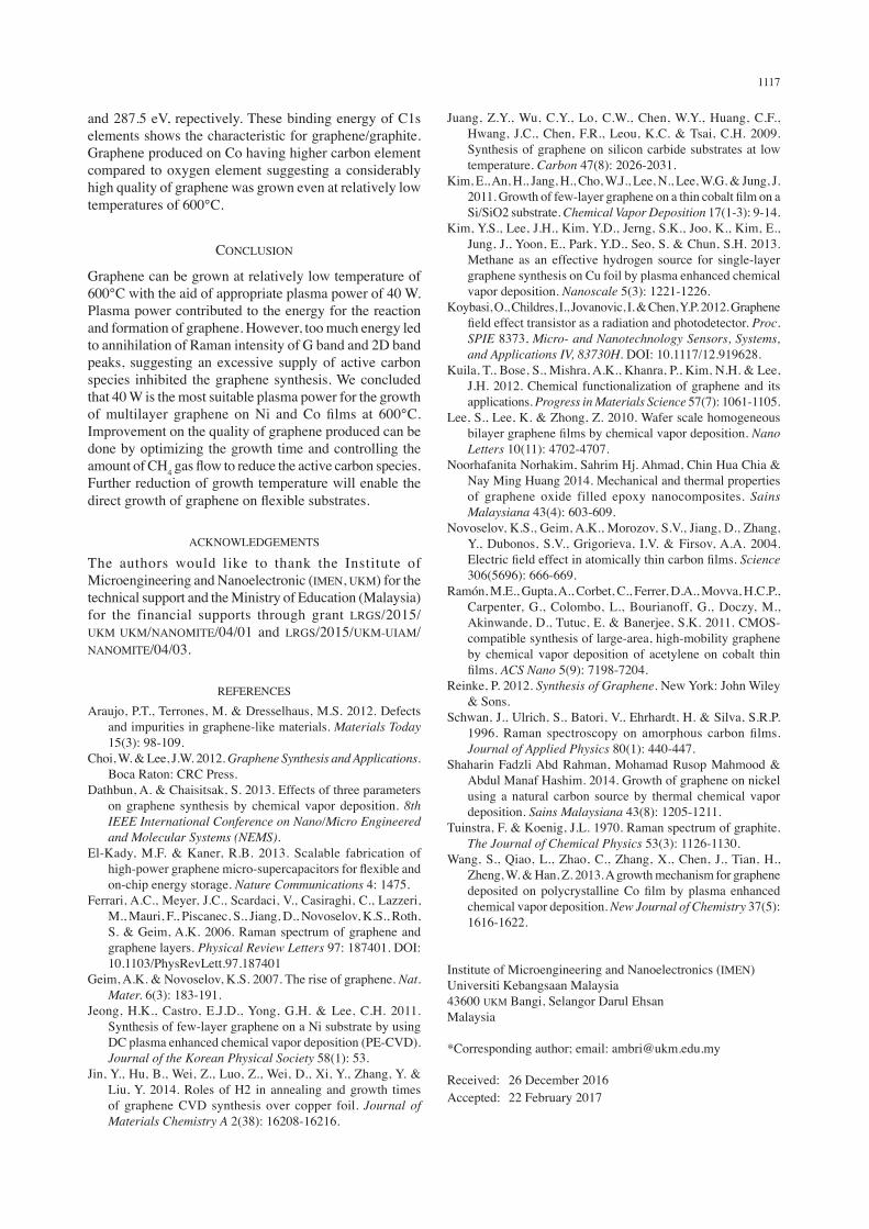
the different surface morphologies during the growth. Most of the multilayer regions exist at metal grain boundaries. Quality of the as-grown graphene was analyzed by characterizing the elements composition using X-ray photoelectron spectroscopy (XPS). Figure 9 exhibits the
XPS spectrum of graphene on Co, showing 2 high peaks that represent C1s and O1s. The C1s and O1s are referred as the carbon element of graphene and the oxygen element on graphene, respectively. By ploting peak below C1s, we identified C-C , C-O and C=O bonding at 284.6, 286
(a) (b)
FIGURE 7. FWHM of 2D peak for graphene growth on (a) Ni and (b) Co at 600°C
FIGURE 9. XPS spectrum of (a) elements in graphene and (b) C1s of as-grown graphene on Co thin film
(a) (b)
FIGURE 8. FESEM images for graphene growth at 40 W on (a) Ni and (b) Co film with magnification of 30 kx
(b)
1117
and 287.5 eV, repectively. These binding energy of C1s elements shows the characteristic for graphene/graphite. Graphene produced on Co having higher carbon element compared to oxygen element suggesting a considerably high quality of graphene was grown even at relatively low temperatures of 600°C.
CONCLUSION
Graphene can be grown at relatively low temperature of 600°C with the aid of appropriate plasma power of 40 W. Plasma power contributed to the energy for the reaction and formation of graphene. However, too much energy led to annihilation of Raman intensity of G band and 2D band peaks, suggesting an excessive supply of active carbon species inhibited the graphene synthesis. We concluded that 40 W is the most suitable plasma power for the growth of multilayer graphene on Ni and Co films at 600°C. Improvement on the quality of graphene produced can be done by optimizing the growth time and controlling the amount of CH4 gas flow to reduce the active carbon species. Further reduction of growth temperature will enable the direct growth of graphene on flexible substrates.
ACKNOWLEDGEMENTS
The authors would like to thank the Institute of Microengineering and Nanoelectronic (IMEN, UKM) for the technical support and the Ministry of Education (Malaysia) for the financial supports through grant LRGS/2015/UKM UKM/NANOMITE/04/01 and LRGS/2015/UKM-UIAM/NANOMITE/04/03.
REFERENCES
Araujo, P.T., Terrones, M. & Dresselhaus, M.S. 2012. Defects and impurities in graphene-like materials. Materials Today 15(3): 98-109.
Choi, W. & Lee, J.W. 2012. Graphene Synthesis and Applications. Boca Raton: CRC Press.
Dathbun, A. & Chaisitsak, S. 2013. Effects of three parameters on graphene synthesis by chemical vapor deposition. 8th IEEE International Conference on Nano/Micro Engineered and Molecular Systems (NEMS).
El-Kady, M.F. & Kaner, R.B. 2013. Scalable fabrication of high-power graphene micro-supercapacitors for flexible and on-chip energy storage. Nature Communications 4: 1475.
Ferrari, A.C., Meyer, J.C., Scardaci, V., Casiraghi, C., Lazzeri, M., Mauri, F., Piscanec, S., Jiang, D., Novoselov, K.S., Roth, S. & Geim, A.K. 2006. Raman spectrum of graphene and graphene layers. Physical Review Letters 97: 187401. DOI: 10.1103/PhysRevLett.97.187401
Geim, A.K. & Novoselov, K.S. 2007. The rise of graphene. Nat. Mater. 6(3): 183-191.
Jeong, H.K., Castro, E.J.D., Yong, G.H. & Lee, C.H. 2011. Synthesis of few-layer graphene on a Ni substrate by using DC plasma enhanced chemical vapor deposition (PE-CVD). Journal of the Korean Physical Society 58(1): 53.
Jin, Y., Hu, B., Wei, Z., Luo, Z., Wei, D., Xi, Y., Zhang, Y. & Liu, Y. 2014. Roles of H2 in annealing and growth times of graphene CVD synthesis over copper foil. Journal of Materials Chemistry A 2(38): 16208-16216.
Juang, Z.Y., Wu, C.Y., Lo, C.W., Chen, W.Y., Huang, C.F., Hwang, J.C., Chen, F.R., Leou, K.C. & Tsai, C.H. 2009. Synthesis of graphene on silicon carbide substrates at low temperature. Carbon 47(8): 2026-2031.
Kim, E., An, H., Jang, H., Cho, W.J., Lee, N., Lee, W.G. & Jung, J. 2011. Growth of few-layer graphene on a thin cobalt film on a Si/SiO2 substrate. Chemical Vapor Deposition 17(1-3): 9-14.
Kim, Y.S., Lee, J.H., Kim, Y.D., Jerng, S.K., Joo, K., Kim, E., Jung, J., Yoon, E., Park, Y.D., Seo, S. & Chun, S.H. 2013. Methane as an effective hydrogen source for single-layer graphene synthesis on Cu foil by plasma enhanced chemical vapor deposition. Nanoscale 5(3): 1221-1226.
Koybasi, O., Childres, I., Jovanovic, I. & Chen, Y.P. 2012. Graphene field effect transistor as a radiation and photodetector. Proc. SPIE 8373, Micro- and Nanotechnology Sensors, Systems, and Applications IV, 83730H. DOI: 10.1117/12.919628.
Kuila, T., Bose, S., Mishra, A.K., Khanra, P., Kim, N.H. & Lee, J.H. 2012. Chemical functionalization of graphene and its applications. Progress in Materials Science 57(7): 1061-1105.
Lee, S., Lee, K. & Zhong, Z. 2010. Wafer scale homogeneous bilayer graphene films by chemical vapor deposition. Nano Letters 10(11): 4702-4707.
Noorhafanita Norhakim, Sahrim Hj. Ahmad, Chin Hua Chia & Nay Ming Huang 2014. Mechanical and thermal properties of graphene oxide filled epoxy nanocomposites. Sains Malaysiana 43(4): 603-609.
Novoselov, K.S., Geim, A.K., Morozov, S.V., Jiang, D., Zhang, Y., Dubonos, S.V., Grigorieva, I.V. & Firsov, A.A. 2004. Electric field effect in atomically thin carbon films. Science 306(5696): 666-669.
Ramón, M.E., Gupta, A., Corbet, C., Ferrer, D.A., Movva, H.C.P., Carpenter, G., Colombo, L., Bourianoff, G., Doczy, M., Akinwande, D., Tutuc, E. & Banerjee, S.K. 2011. CMOS-compatible synthesis of large-area, high-mobility graphene by chemical vapor deposition of acetylene on cobalt thin films. ACS Nano 5(9): 7198-7204.
Reinke, P. 2012. Synthesis of Graphene. New York: John Wiley & Sons.
Schwan, J., Ulrich, S., Batori, V., Ehrhardt, H. & Silva, S.R.P. 1996. Raman spectroscopy on amorphous carbon films. Journal of Applied Physics 80(1): 440-447.
Shaharin Fadzli Abd Rahman, Mohamad Rusop Mahmood & Abdul Manaf Hashim. 2014. Growth of graphene on nickel using a natural carbon source by thermal chemical vapor deposition. Sains Malaysiana 43(8): 1205-1211.
Tuinstra, F. & Koenig, J.L. 1970. Raman spectrum of graphite. The Journal of Chemical Physics 53(3): 1126-1130.
Wang, S., Qiao, L., Zhao, C., Zhang, X., Chen, J., Tian, H., Zheng, W. & Han, Z. 2013. A growth mechanism for graphene deposited on polycrystalline Co film by plasma enhanced chemical vapor deposition. New Journal of Chemistry 37(5): 1616-1622.
Institute of Microengineering and Nanoelectronics (IMEN)Universiti Kebangsaan Malaysia 43600 UKM Bangi, Selangor Darul EhsanMalaysia
*Corresponding author; email: [email protected]
Received: 26 December 2016Accepted: 22 February 2017
(a) (b)
FIGURE 8. FESEM images for graphene growth at 40 W on (a) Ni and (b) Co film with magnification of 30 kx
(b)