communication fabrication and characterization of near
TRANSCRIPT
Communication
Fabrication and Characterization of Near Infrared
Molybdenum Disulfide/Silicon Heterojunction Photodetector
by Drop Casting Method
Haroon Rashid 1,*, Norhana Arsad 1,*, Harith Ahmad 2,3, Ahmad Ashrif A. Bakar 1 and Mamun Ibne Reaz 1,*
1 Department of Electrical, Electronic and Systems Engineering, Faculty of Engineering and Built Environ-
ment, Universiti Kebangsaan Malaysia, 43600 UKM Bangi, Selangor, Malaysia; [email protected] (H.R.);
[email protected] (N.A.); [email protected] (A.A.A.B); [email protected] (M.I.R.) 2 Photonics Research Centre, University of Malaya, 50603 Kuala Lumpur, Malaysia 3 Department of Physics, Faculty of Science, University of Malaya, 50603 Kuala Lumpur, Malaysia
* Correspondence: [email protected] (H.R.); [email protected] (N.A.); [email protected] (M.I.R.)
Abstract: In this work, a highly efficient, molybdenum disulfide (MoS2) based near infrared (NIR)
heterojunction photodetector is fabricated on a Si substrate using a cost-effective and simple drop
casting method. A non-stoichiometric and inhomogeneous MoS2 layer with a S/Mo ratio of 2.02 is
detected using energy dispersive X-ray spectroscopy and field emission scanning electron micro-
scope analysis. Raman shifts are noticed at 382.42 cm-1 and 407.97 cm-1, validating MoS2 thin film
growth with a direct bandgap of 2.01 eV. The fabricated n-MoS2/p-Si photodetector is illuminated
with a 785 nm laser at different intensities, and demonstrate the ability of the photodetector to work
in both regions, the forward biased and reverse biased from above 1.5 V and less than -1.0 V. The
highest responsivity, R is calculated to be 0.52 A/W while the detectivity D* is 4.08 x 10¹⁰ Jones for
an incident light intensity of 9.57 mW/cm2. The minimum rise and fall times are calculated as 1.77
ms and 1.31 ms for an incident laser power of 9.57 mW/cm2 and 6.99 mW/cm2 respectively at a direct
current bias voltage of 10 V. The demonstrated results are promising for the low-cost fabrication of
a thin MoS2 film for photonics and optoelectronic device applications.
Keywords: MoS2; photodetector; Raman; drop casting; infrared; thin film
1. Introduction
Transition metal di chalcogenides (TMDC) have recently drawn a lot of interest ow-
ing to their exceptional optical and electronic properties, which give them value for opto-
electronic applications. TMDC have a typical structure of MX2, where M being a transition
metal, commonly Mo and W and X being a chalcogen such as S and Se. Amongst these
TMDC, MoS2 has the layered structure of S-Mo-S with one Mo atom covalently bonded to
two S atoms. Furthermore, MoS2 has a particular advantage over graphene in that gra-
phene has a zero bandgap, while monolayer MoS2 has an indirect bandgap of 1.29 eV and
direct transition starts from 1.8 eV. Also, it has stable crystalline structure, size dependent
bandgap and found in either semiconductor or metallic nature. It is widely reported in
various applications ranging from sensors, transistors, and solar cells to optical fiber lasers
and photodetectors 1-10.
MoS2 can be synthesized using a variety of techniques, depending on the properties
that the application requires. In its bulk form, these 2D materials have weak Van der
Waals forces between the layers, and as such mechanical exfoliation has been an easy and
common method of obtaining 2D material films that are a few layers in thickness. In fact,
the use of scotch tape has been reported extensively as a simple method of obtaining a
MoS2 film that are only a few layers thick, but not appropriate for sizable production due
to its inability to control the shape of the flakes obtained, nor their thickness and size 11. In
anticipation of a single atomic layer, or two to three layers thick MoS2 films, liquid
Preprints (www.preprints.org) | NOT PEER-REVIEWED | Posted: 5 April 2021 doi:10.20944/preprints202104.0119.v1
© 2021 by the author(s). Distributed under a Creative Commons CC BY license.
exfoliation is instead used. Also, ultra-thin layers are obtained by the sonication of an ex-
foliated solvent. The drawback of this approach however is that the process can cause
defects in the fabricated layers and reduce the number of layers obtained, thus limiting its
applications 12, 13. Another widely used method to obtain thin MoS2 layers is chemical va-
por deposition (CVD) where atomically thin layers can be synthesized by thermal evapo-
ration or sulfurization on a precursor reagent such as Mo14, MoO2 and MoO3 15, 16. However
by using this approach, the obtained films are polycrystalline in nature and incorporate
small crystallite deposits, making it difficult to control the layers 17, 18. In this regard, the
drop casting method has become a popular technique for depositing MoS2 layers onto a
photonic surface due to simplicity, high stability, and reproducibility for larger scale pro-
duction. Significant reports have already demonstrated the potential of this fabrication
method, capable of generating highly stable, reproducible, and efficient thin films 19-22.
In the development of photodetectors, 2D materials play a vital role in increasing the
performance and reliability of the photodetector. In this regard, the number of MoS2 layers
has a great impact on the performance of the photodetector. Mechanically exfoliated sin-
gle, double, and triple layers of MoS2, labelled as 1L, 2L and 3L respectively are used to
fabricate a phototransistor with the reported optical bandgap for the 1L being 1.82 eV, 1.65
eV for the 2L and 1.35 eV for the 3L. The fabricated devices based on the 1L and 2L have
high performance detection under green light illumination while the 3L based photode-
tector is only sensitive when illuminated by under the red wavelength region 23. A reduced
bandgap allows for the detection of light across a wider range of wavelength, and closer
to the near infrared (NIR) region for MoS2 multiple layers thick. Similarly, ultraviolet (UV)
to infrared (IR) photo-detection has been reported previously using thin films obtained
by mechanical exfoliation 24. Moreover, NIR photodetector has also been realized by
multi-layer MoS2 flakes obtained via chemical exfoliation 25. Recently, a broadband UV-
visible-NIR (UV-Vis-NIR) photodetector using the aforementioned 2D material is re-
ported, with a detectivity of 1010 Jones and a responsivity of 0.0084 A/W that demonstrates
good performance 26.
In this work, a low-cost and highly efficient heterojunction photodetector device us-
ing MoS2 thin film deposited on the surface of a Si substrate by drop casting technique is
proposed and demonstrated. The n-MoS2/p-Si photodetector device is characterized for
its structural, optical, morphological, and compositional properties by Raman, photolu-
minescence (PL), field emission scanning electron microscope (FESEM) and energy dis-
persive X-ray (EDX) spectroscopy, respectively. The device is further characterized for its
optoelectronic properties by current-voltage (IV) measurement system under illumination
and dark conditions using a 785 nm near infrared (NIR) light source.
2. Materials and Methods
2.1. Device Fabrication
The MoS2 based heterojunction photodetector device is fabricated employing the
drop casting technique. The boron (B) doped crystalline silicon (c-Si) wafer is used as the
p-type substrate in this device configuration. A thin layer of MoS2 serves as the n-type
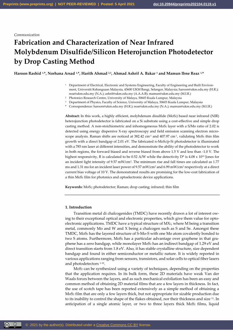
layer to establish a heterojunction with p-Si, as revealed in Figure 1.
Figure 1. Schematic diagram of drop-casting thin MoS2 layer on top of p-Si substrate.
The pristine MoS2 nano-flakes are obtained from the Graphene Supermarket in an
ethanol/deionized (DI) water solution. The pristine nano-flakes have a concentration of 18
Preprints (www.preprints.org) | NOT PEER-REVIEWED | Posted: 5 April 2021 doi:10.20944/preprints202104.0119.v1
mg/L with a lateral size of 100 nm - 400 nm. The MoS2 solution is first sonicated for 30 min
at 80 ℃ and at the same time the p-Si wafer is cut into 3 cm x 2 cm rectangular shape. The
substrate on the other hand is cleansed ultrasonically using isopropyl alcohol (IPA) and
deionized (DI) water for 20 and 30 min respectively to eliminate any contaminants from
the surface before being dried using pure nitrogen (N2) gas. Subsequently, a hotplate is
heated to 60℃ and the substrate is placed on top of it for pre-deposition heating for 5 min.
Approximately 5 µl of the MoS2 solution using a micropipette is drop casted onto the sur-
face of the p-Si substrate. After about 5 min, the sample is removed from the hotplate and
kept in a desiccator for 24 hrs. to dry naturally. Finally, the electrodes are formed by silver
(Ag) paste deposited on both the p-Si and n-MoS2 surfaces to form the conductive contacts.
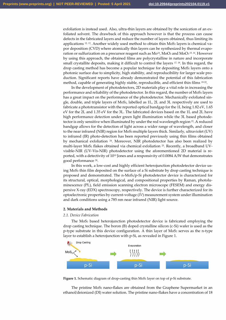
The schematic diagram of the fabricated heterojunction device is presented in Figure 2 (a).
Figure 2. (a) Schematic diagram of fabricated n-MoS2/p-Si heterojunction photodetector. (b) En-
ergy band diagram of n-MoS2/p-Si in isolated state.
2.2. Characterization & Device Measurement
The surface morphology of the fabricated device is obtained using a JEOL JSM7600F
FESEM, while compositional analysis and mapping are performed using an Oxford In-
struments EDX. An inVia confocal Raman microscope with 532 nm illumination is used
to obtain the elemental composition of the heterojunction device. The optoelectronic char-
acteristics of the heterojunction n-MoS2/p-Si photodetector is measured under 785 nm il-
lumination at the NIR region. A Keithley 2410 – 1100 V SourceMeter® is used to obtain
the IV curves between -10 V to 10 V. The distance from the surface of photodetector to the
laser source is kept constant at 2 cm and the effective area (A) is calculated to be 0.0706
cm2. The power densities of the illumination source are varied (6.06 mW/cm2, 6.99
mW/cm2, 8.05 mW/cm2 and 9.57 mW/cm2). The photodetector’s time-based responses are
collected using a Yokogawa DLM2054 mixed signal oscilloscope. The bias voltages (VB)
are varied from 1.0 V to 10.0 V with an interval of 1.0 V. The Stanford Research Systems’
DS345 – 30 MHz synthesized function generator (SFG) is used to modulate frequency sig-
nals from 1 Hz to 20 kHz for testing the photodetector. All the measurements are obtained
at the ambient conditions.
3. Results & Discussion
3.1. Raman & Photoluminescence
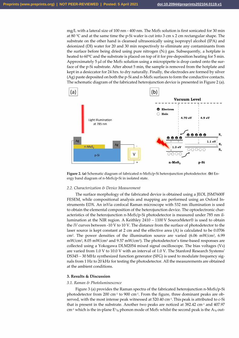
Figure 3 (a) provides the Raman spectra of the fabricated heterojunction n-MoS2/p-Si
photodetector from 200 cm-1 to 900 cm-1. From the figure, three dominant peaks are ob-
served, with the most intense peak witnessed at 520.40 cm-1. This peak is attributed to c-Si
that is present in the substrate. Another two peaks are noticed at 382.42 cm-1 and 407.97
cm-1 which is the in-plane E12g phonon mode of MoS2 whilst the second peak is the A1g out-
Preprints (www.preprints.org) | NOT PEER-REVIEWED | Posted: 5 April 2021 doi:10.20944/preprints202104.0119.v1
plane mode. These two peaks confirm the successful development of MoS2 thin film 27.
The distance (Δ) between the modes is calculated to be nearly 25.55 cm-1 with the weak
van der Waals interlayer forces between the sulfur (S) atoms in particular resulting in the
lattice vibrations. These findings are consistent with previous research 28. The photolumi-
nescence (PL) spectra of the MoS2 is given in Figure 3 (b) and from this the energy bandgap
is calculated. A direct bandgap of 2.01 eV is obtained, indicating the successful deposition
of a n-type MoS2 thin film from the drop casting technique 29, 30.
Figure 3. (a) Raman spectra of heterojunction n-MoS2/p-Si photodetector device and (b) PL spectra
with respect to energy bandgap of MoS2 thin film.
3.2. FESEM & EDX
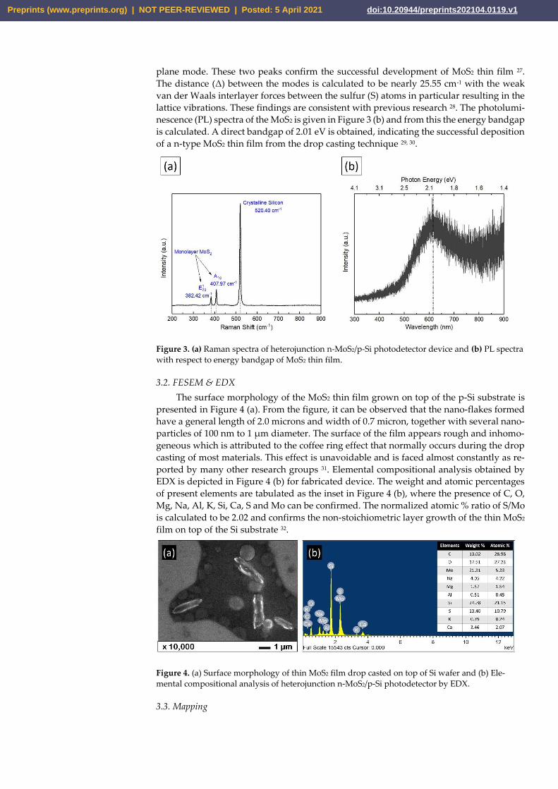
The surface morphology of the MoS2 thin film grown on top of the p-Si substrate is
presented in Figure 4 (a). From the figure, it can be observed that the nano-flakes formed
have a general length of 2.0 microns and width of 0.7 micron, together with several nano-
particles of 100 nm to 1 µm diameter. The surface of the film appears rough and inhomo-
geneous which is attributed to the coffee ring effect that normally occurs during the drop
casting of most materials. This effect is unavoidable and is faced almost constantly as re-
ported by many other research groups 31. Elemental compositional analysis obtained by
EDX is depicted in Figure 4 (b) for fabricated device. The weight and atomic percentages
of present elements are tabulated as the inset in Figure 4 (b), where the presence of C, O,
Mg, Na, Al, K, Si, Ca, S and Mo can be confirmed. The normalized atomic % ratio of S/Mo
is calculated to be 2.02 and confirms the non-stoichiometric layer growth of the thin MoS2
film on top of the Si substrate 32.
Figure 4. (a) Surface morphology of thin MoS2 film drop casted on top of Si wafer and (b) Ele-
mental compositional analysis of heterojunction n-MoS2/p-Si photodetector by EDX.
3.3. Mapping
Preprints (www.preprints.org) | NOT PEER-REVIEWED | Posted: 5 April 2021 doi:10.20944/preprints202104.0119.v1
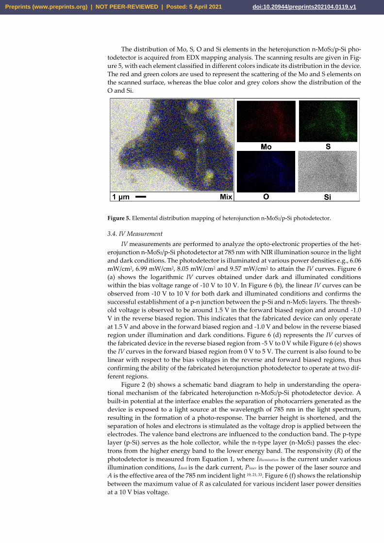
The distribution of Mo, S, O and Si elements in the heterojunction n-MoS2/p-Si pho-
todetector is acquired from EDX mapping analysis. The scanning results are given in Fig-
ure 5, with each element classified in different colors indicate its distribution in the device.
The red and green colors are used to represent the scattering of the Mo and S elements on
the scanned surface, whereas the blue color and grey colors show the distribution of the
O and Si.
Figure 5. Elemental distribution mapping of heterojunction n-MoS2/p-Si photodetector.
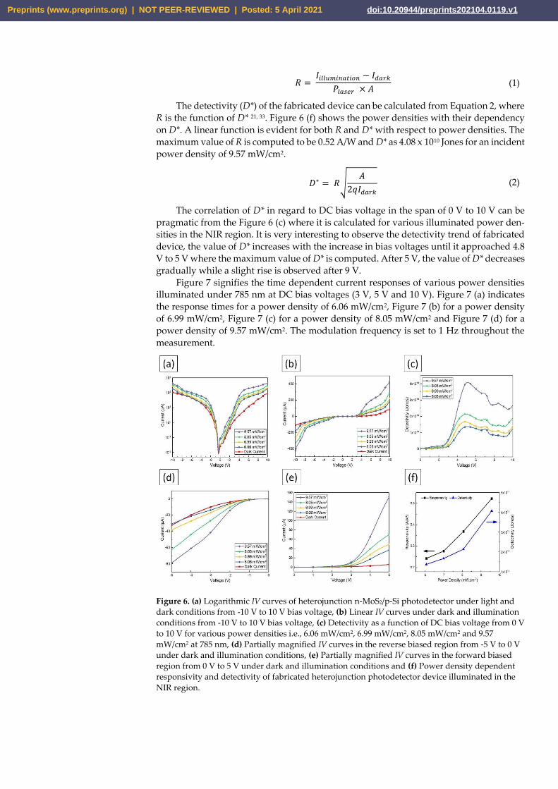
3.4. IV Measurement
IV measurements are performed to analyze the opto-electronic properties of the het-
erojunction n-MoS2/p-Si photodetector at 785 nm with NIR illumination source in the light
and dark conditions. The photodetector is illuminated at various power densities e.g., 6.06
mW/cm2, 6.99 mW/cm2, 8.05 mW/cm2 and 9.57 mW/cm2 to attain the IV curves. Figure 6
(a) shows the logarithmic IV curves obtained under dark and illuminated conditions
within the bias voltage range of -10 V to 10 V. In Figure 6 (b), the linear IV curves can be
observed from -10 V to 10 V for both dark and illuminated conditions and confirms the
successful establishment of a p-n junction between the p-Si and n-MoS2 layers. The thresh-
old voltage is observed to be around 1.5 V in the forward biased region and around -1.0
V in the reverse biased region. This indicates that the fabricated device can only operate
at 1.5 V and above in the forward biased region and -1.0 V and below in the reverse biased
region under illumination and dark conditions. Figure 6 (d) represents the IV curves of
the fabricated device in the reverse biased region from -5 V to 0 V while Figure 6 (e) shows
the IV curves in the forward biased region from 0 V to 5 V. The current is also found to be
linear with respect to the bias voltages in the reverse and forward biased regions, thus
confirming the ability of the fabricated heterojunction photodetector to operate at two dif-
ferent regions.
Figure 2 (b) shows a schematic band diagram to help in understanding the opera-
tional mechanism of the fabricated heterojunction n-MoS2/p-Si photodetector device. A
built-in potential at the interface enables the separation of photocarriers generated as the
device is exposed to a light source at the wavelength of 785 nm in the light spectrum,
resulting in the formation of a photo-response. The barrier height is shortened, and the
separation of holes and electrons is stimulated as the voltage drop is applied between the
electrodes. The valence band electrons are influenced to the conduction band. The p-type
layer (p-Si) serves as the hole collector, while the n-type layer (n-MoS2) passes the elec-
trons from the higher energy band to the lower energy band. The responsivity (R) of the
photodetector is measured from Equation 1, where Iillumination is the current under various
illumination conditions, Idark is the dark current, Plaser is the power of the laser source and
A is the effective area of the 785 nm incident light 19, 21, 33. Figure 6 (f) shows the relationship
between the maximum value of R as calculated for various incident laser power densities
at a 10 V bias voltage.
Preprints (www.preprints.org) | NOT PEER-REVIEWED | Posted: 5 April 2021 doi:10.20944/preprints202104.0119.v1
𝑅 = 𝐼𝑖𝑙𝑙𝑢𝑚𝑖𝑛𝑎𝑡𝑖𝑜𝑛 − 𝐼𝑑𝑎𝑟𝑘
𝑃𝑙𝑎𝑠𝑒𝑟 × 𝐴 (1)
The detectivity (D*) of the fabricated device can be calculated from Equation 2, where
R is the function of D* 21, 33. Figure 6 (f) shows the power densities with their dependency
on D*. A linear function is evident for both R and D* with respect to power densities. The
maximum value of R is computed to be 0.52 A/W and D* as 4.08 x 10¹⁰ Jones for an incident
power density of 9.57 mW/cm2.
𝐷∗ = 𝑅√𝐴
2𝑞𝐼𝑑𝑎𝑟𝑘
(2)
The correlation of D* in regard to DC bias voltage in the span of 0 V to 10 V can be
pragmatic from the Figure 6 (c) where it is calculated for various illuminated power den-
sities in the NIR region. It is very interesting to observe the detectivity trend of fabricated
device, the value of D* increases with the increase in bias voltages until it approached 4.8
V to 5 V where the maximum value of D* is computed. After 5 V, the value of D* decreases
gradually while a slight rise is observed after 9 V.
Figure 7 signifies the time dependent current responses of various power densities
illuminated under 785 nm at DC bias voltages (3 V, 5 V and 10 V). Figure 7 (a) indicates
the response times for a power density of 6.06 mW/cm2, Figure 7 (b) for a power density
of 6.99 mW/cm2, Figure 7 (c) for a power density of 8.05 mW/cm2 and Figure 7 (d) for a
power density of 9.57 mW/cm2. The modulation frequency is set to 1 Hz throughout the
measurement.
Figure 6. (a) Logarithmic IV curves of heterojunction n-MoS2/p-Si photodetector under light and
dark conditions from -10 V to 10 V bias voltage, (b) Linear IV curves under dark and illumination
conditions from -10 V to 10 V bias voltage, (c) Detectivity as a function of DC bias voltage from 0 V
to 10 V for various power densities i.e., 6.06 mW/cm2, 6.99 mW/cm2, 8.05 mW/cm2 and 9.57
mW/cm2 at 785 nm, (d) Partially magnified IV curves in the reverse biased region from -5 V to 0 V
under dark and illumination conditions, (e) Partially magnified IV curves in the forward biased
region from 0 V to 5 V under dark and illumination conditions and (f) Power density dependent
responsivity and detectivity of fabricated heterojunction photodetector device illuminated in the
NIR region.
Preprints (www.preprints.org) | NOT PEER-REVIEWED | Posted: 5 April 2021 doi:10.20944/preprints202104.0119.v1
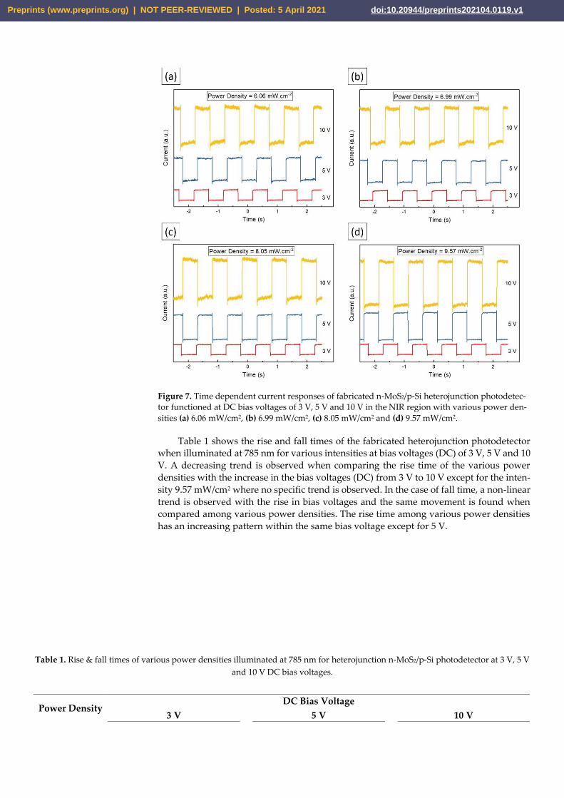
Figure 7. Time dependent current responses of fabricated n-MoS2/p-Si heterojunction photodetec-
tor functioned at DC bias voltages of 3 V, 5 V and 10 V in the NIR region with various power den-
sities (a) 6.06 mW/cm2, (b) 6.99 mW/cm2, (c) 8.05 mW/cm2 and (d) 9.57 mW/cm2.
Table 1 shows the rise and fall times of the fabricated heterojunction photodetector
when illuminated at 785 nm for various intensities at bias voltages (DC) of 3 V, 5 V and 10
V. A decreasing trend is observed when comparing the rise time of the various power
densities with the increase in the bias voltages (DC) from 3 V to 10 V except for the inten-
sity 9.57 mW/cm2 where no specific trend is observed. In the case of fall time, a non-linear
trend is observed with the rise in bias voltages and the same movement is found when
compared among various power densities. The rise time among various power densities
has an increasing pattern within the same bias voltage except for 5 V.
Table 1. Rise & fall times of various power densities illuminated at 785 nm for heterojunction n-MoS2/p-Si photodetector at 3 V, 5 V
and 10 V DC bias voltages.
Power Density DC Bias Voltage
3 V
5 V
10 V
Preprints (www.preprints.org) | NOT PEER-REVIEWED | Posted: 5 April 2021 doi:10.20944/preprints202104.0119.v1
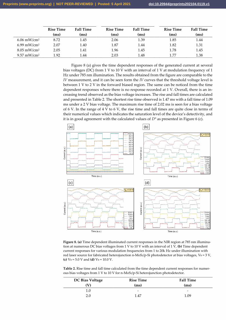
Figure 8 (a) gives the time dependent responses of the generated current at several
bias voltages (DC) from 1 V to 10 V with an interval of 1 V at modulation frequency of 1
Hz under 785 nm illumination. The results obtained from the figure are comparable to the
IV measurement, and it can be seen form the IV curves that the threshold voltage level is
between 1 V to 2 V in the forward biased region. The same can be noticed from the time
dependent responses where there is no response recorded at 1 V. Overall, there is an in-
creasing trend observed as the bias voltage increases. The rise and fall times are calculated
and presented in Table 2. The shortest rise time observed is 1.47 ms with a fall time of 1.09
ms under a 2 V bias voltage. The maximum rise time of 2.02 ms is seen for a bias voltage
of 6 V. In the range of 4 V to 6 V, the rise time and fall times are quite close in terms of
their numerical values which indicates the saturation level of the device’s detectivity, and
it is in good agreement with the calculated values of D* as presented in Figure 6 (c).
Figure 8. (a) Time dependent illuminated current responses in the NIR region at 785 nm illumina-
tion at numerous DC bias voltages from 1 V to 10 V with an interval of 1 V, (b) Time dependent
current responses for various modulation frequencies from 1 to 20k Hz under illumination with
red laser source for fabricated heterojunction n-MoS2/p-Si photodetector at bias voltages, VB = 3 V,
(c) VB = 5.0 V and (d) VB = 10.0 V.
Table 2. Rise time and fall time calculated from the time dependent current responses for numer-
ous bias voltages from 1 V to 10 V for n-MoS2/p-Si heterojunction photodetector.
DC Bias Voltage
(V)
Rise Time
(ms)
Fall Time
(ms)
1.0 - -
2.0 1.47 1.09
Rise Time
(ms)
Fall Time
(ms)
Rise Time
(ms)
Fall Time
(ms)
Rise Time
(ms)
Fall Time
(ms)
6.06 mW/cm2 8.72 1.45
2.06 1.39
1.85 1.44
6.99 mW/cm2 2.07 1.40
1.87 1.44
1.82 1.31
8.05 mW/cm2 2.05 1.41
1.96 1.45
1.78 1.45
9.57 mW/cm2 1.92 1.44
2.03 1.48
1.77 1.38
Preprints (www.preprints.org) | NOT PEER-REVIEWED | Posted: 5 April 2021 doi:10.20944/preprints202104.0119.v1
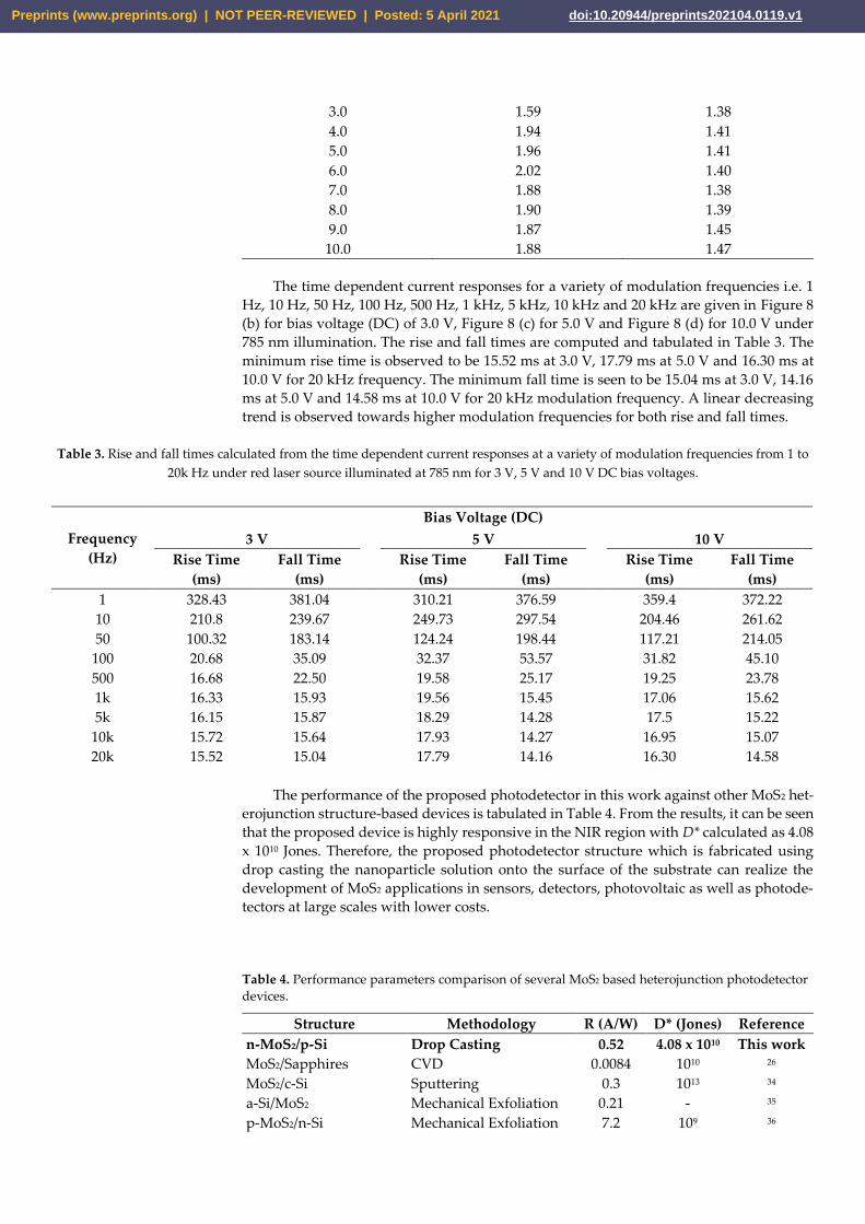
3.0 1.59 1.38
4.0 1.94 1.41
5.0 1.96 1.41
6.0 2.02 1.40
7.0 1.88 1.38
8.0 1.90 1.39
9.0 1.87 1.45
10.0 1.88 1.47
The time dependent current responses for a variety of modulation frequencies i.e. 1
Hz, 10 Hz, 50 Hz, 100 Hz, 500 Hz, 1 kHz, 5 kHz, 10 kHz and 20 kHz are given in Figure 8
(b) for bias voltage (DC) of 3.0 V, Figure 8 (c) for 5.0 V and Figure 8 (d) for 10.0 V under
785 nm illumination. The rise and fall times are computed and tabulated in Table 3. The
minimum rise time is observed to be 15.52 ms at 3.0 V, 17.79 ms at 5.0 V and 16.30 ms at
10.0 V for 20 kHz frequency. The minimum fall time is seen to be 15.04 ms at 3.0 V, 14.16
ms at 5.0 V and 14.58 ms at 10.0 V for 20 kHz modulation frequency. A linear decreasing
trend is observed towards higher modulation frequencies for both rise and fall times.
Table 3. Rise and fall times calculated from the time dependent current responses at a variety of modulation frequencies from 1 to
20k Hz under red laser source illuminated at 785 nm for 3 V, 5 V and 10 V DC bias voltages.
The performance of the proposed photodetector in this work against other MoS2 het-
erojunction structure-based devices is tabulated in Table 4. From the results, it can be seen
that the proposed device is highly responsive in the NIR region with D* calculated as 4.08
x 1010 Jones. Therefore, the proposed photodetector structure which is fabricated using
drop casting the nanoparticle solution onto the surface of the substrate can realize the
development of MoS2 applications in sensors, detectors, photovoltaic as well as photode-
tectors at large scales with lower costs.
Table 4. Performance parameters comparison of several MoS2 based heterojunction photodetector
devices.
Structure Methodology R (A/W) D* (Jones) Reference
n-MoS2/p-Si Drop Casting 0.52 4.08 x 10¹⁰ This work
MoS2/Sapphires CVD 0.0084 1010 26
MoS2/c-Si Sputtering 0.3 1013 34
a-Si/MoS2 Mechanical Exfoliation 0.21 - 35
p-MoS2/n-Si Mechanical Exfoliation 7.2 109 36
Frequency
(Hz)
Bias Voltage (DC)
3 V
5 V
10 V
Rise Time
(ms)
Fall Time
(ms)
Rise Time
(ms)
Fall Time
(ms)
Rise Time
(ms)
Fall Time
(ms)
1 328.43 381.04
310.21 376.59
359.4 372.22
10 210.8 239.67
249.73 297.54
204.46 261.62
50 100.32 183.14
124.24 198.44
117.21 214.05
100 20.68 35.09
32.37 53.57
31.82 45.10
500 16.68 22.50
19.58 25.17
19.25 23.78
1k 16.33 15.93
19.56 15.45
17.06 15.62
5k 16.15 15.87
18.29 14.28
17.5 15.22
10k 15.72 15.64
17.93 14.27
16.95 15.07
20k 15.52 15.04
17.79 14.16
16.30 14.58
Preprints (www.preprints.org) | NOT PEER-REVIEWED | Posted: 5 April 2021 doi:10.20944/preprints202104.0119.v1
MoS2/Flat GaN CVD and Transfer 0.16 - 37
MoS2/Patterned GaN CVD and Transfer 0.25 5.6 x 10⁸ 37
Au-NPS/MoS2 Hydrothermal 0.04603 - 38
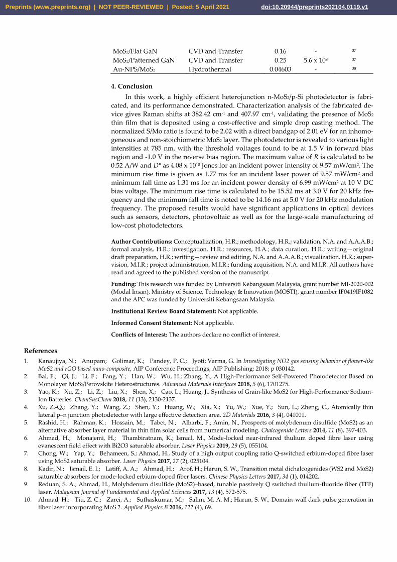
4. Conclusion
In this work, a highly efficient heterojunction n-MoS2/p-Si photodetector is fabri-
cated, and its performance demonstrated. Characterization analysis of the fabricated de-
vice gives Raman shifts at 382.42 cm-1 and 407.97 cm-1, validating the presence of MoS2
thin film that is deposited using a cost-effective and simple drop casting method. The
normalized S/Mo ratio is found to be 2.02 with a direct bandgap of 2.01 eV for an inhomo-
geneous and non-stoichiometric MoS2 layer. The photodetector is revealed to various light
intensities at 785 nm, with the threshold voltages found to be at 1.5 V in forward bias
region and -1.0 V in the reverse bias region. The maximum value of R is calculated to be
0.52 A/W and D* as 4.08 x 10¹⁰ Jones for an incident power intensity of 9.57 mW/cm2. The
minimum rise time is given as 1.77 ms for an incident laser power of 9.57 mW/cm2 and
minimum fall time as 1.31 ms for an incident power density of 6.99 mW/cm2 at 10 V DC
bias voltage. The minimum rise time is calculated to be 15.52 ms at 3.0 V for 20 kHz fre-
quency and the minimum fall time is noted to be 14.16 ms at 5.0 V for 20 kHz modulation
frequency. The proposed results would have significant applications in optical devices
such as sensors, detectors, photovoltaic as well as for the large-scale manufacturing of
low-cost photodetectors.
Author Contributions: Conceptualization, H.R.; methodology, H.R.; validation, N.A. and A.A.A.B.;
formal analysis, H.R.; investigation, H.R.; resources, H.A.; data curation, H.R.; writing—original
draft preparation, H.R.; writing—review and editing, N.A. and A.A.A.B.; visualization, H.R.; super-
vision, M.I.R.; project administration, M.I.R.; funding acquisition, N.A. and M.I.R. All authors have
read and agreed to the published version of the manuscript.
Funding: This research was funded by Universiti Kebangsaan Malaysia, grant number MI-2020-002
(Modal Insan), Ministry of Science, Technology & Innovation (MOSTI), grant number IF0419IF1082
and the APC was funded by Universiti Kebangsaan Malaysia.
Institutional Review Board Statement: Not applicable.
Informed Consent Statement: Not applicable.
Conflicts of Interest: The authors declare no conflict of interest.
References
1. Kanaujiya, N.; Anupam; Golimar, K.; Pandey, P. C.; Jyoti; Varma, G. In Investigating NO2 gas sensing behavior of flower-like
MoS2 and rGO based nano-composite, AIP Conference Proceedings, AIP Publishing: 2018; p 030142.
2. Bai, F.; Qi, J.; Li, F.; Fang, Y.; Han, W.; Wu, H.; Zhang, Y., A High‐Performance Self‐Powered Photodetector Based on
Monolayer MoS2/Perovskite Heterostructures. Advanced Materials Interfaces 2018, 5 (6), 1701275.
3. Yao, K.; Xu, Z.; Li, Z.; Liu, X.; Shen, X.; Cao, L.; Huang, J., Synthesis of Grain‐like MoS2 for High‐Performance Sodium‐
Ion Batteries. ChemSusChem 2018, 11 (13), 2130-2137.
4. Xu, Z.-Q.; Zhang, Y.; Wang, Z.; Shen, Y.; Huang, W.; Xia, X.; Yu, W.; Xue, Y.; Sun, L.; Zheng, C., Atomically thin
lateral p–n junction photodetector with large effective detection area. 2D Materials 2016, 3 (4), 041001.
5. Rashid, H.; Rahman, K.; Hossain, M.; Tabet, N.; Alharbi, F.; Amin, N., Prospects of molybdenum disulfide (MoS2) as an
alternative absorber layer material in thin film solar cells from numerical modeling. Chalcogenide Letters 2014, 11 (8), 397-403.
6. Ahmad, H.; Monajemi, H.; Thambiratnam, K.; Ismail, M., Mode-locked near-infrared thulium doped fibre laser using
evanescent field effect with Bi2O3 saturable absorber. Laser Physics 2019, 29 (5), 055104.
7. Chong, W.; Yap, Y.; Behameen, S.; Ahmad, H., Study of a high output coupling ratio Q-switched erbium-doped fibre laser
using MoS2 saturable absorber. Laser Physics 2017, 27 (2), 025104.
8. Kadir, N.; Ismail, E. I.; Latiff, A. A.; Ahmad, H.; Arof, H.; Harun, S. W., Transition metal dichalcogenides (WS2 and MoS2)
saturable absorbers for mode-locked erbium-doped fiber lasers. Chinese Physics Letters 2017, 34 (1), 014202.
9. Reduan, S. A.; Ahmad, H., Molybdenum disulfide (MoS2)–based, tunable passively Q switched thulium-fluoride fiber (TFF)
laser. Malaysian Journal of Fundamental and Applied Sciences 2017, 13 (4), 572-575.
10. Ahmad, H.; Tiu, Z. C.; Zarei, A.; Suthaskumar, M.; Salim, M. A. M.; Harun, S. W., Domain-wall dark pulse generation in
fiber laser incorporating MoS 2. Applied Physics B 2016, 122 (4), 69.
Preprints (www.preprints.org) | NOT PEER-REVIEWED | Posted: 5 April 2021 doi:10.20944/preprints202104.0119.v1
11. Novoselov, K. S.; Geim, A. K.; Morozov, S. V.; Jiang, D.; Zhang, Y.; Dubonos, S. V.; Grigorieva, I. V.; Firsov, A. A.,
Electric field effect in atomically thin carbon films. science 2004, 306 (5696), 666-669.
12. Zeng, Z.; Yin, Z.; Huang, X.; Li, H.; He, Q.; Lu, G.; Boey, F.; Zhang, H., Single‐Layer Semiconducting Nanosheets: High‐
yield preparation and device fabrication. Angewandte Chemie International Edition 2011, 50 (47), 11093-11097.
13. Ambrosi, A.; Sofer, Z.; Pumera, M., Lithium intercalation compound dramatically influences the electrochemical properties of
exfoliated MoS2. Small 2015, 11 (5), 605-612.
14. Rashid, H.; Rahman, K. S.; Hossain, M. I.; Nasser, A. A.; Alharbi, F. H.; Akhtaruzzaman, M.; Amin, N., Physical and
electrical properties of molybdenum thin films grown by DC magnetron sputtering for photovoltaic application. Results in
Physics 2019, 14, 102515.
15. Chelvanathan, P.; Rahman, K. S.; Hossain, M. I.; Rashid, H.; Samsudin, N.; Mustafa, S. N.; Bais, B.; Akhtaruzzaman,
M.; Amin, N., Growth of MoOx nanobelts from molybdenum bi-layer thin films for thin film solar cell application. Thin Solid
Films 2017, 621, 240-246.
16. Rosman, N. N.; Yunus, R. M.; Minggu, L. J.; Arifin, K.; Kassim, M. B.; Mohamed, M. A. J. J. T., Chemical vapor deposition
growth of molybdenum disulfide for photoelectrochemical hydrogen generation. 2020, 26, 68-74.
17. Lin, Y.-C.; Zhang, W.; Huang, J.-K.; Liu, K.-K.; Lee, Y.-H.; Liang, C.-T.; Chu, C.-W.; Li, L.-J., Wafer-scale MoS 2 thin
layers prepared by MoO 3 sulfurization. Nanoscale 2012, 4 (20), 6637-6641.
18. Balendhran, S.; Ou, J. Z.; Bhaskaran, M.; Sriram, S.; Ippolito, S.; Vasic, Z.; Kats, E.; Bhargava, S.; Zhuiykov, S.;
Kalantar-Zadeh, K., Atomically thin layers of MoS 2 via a two step thermal evaporation–exfoliation method. Nanoscale 2012, 4
(2), 461-466.
19. Ahmad, H.; Rashid, H.; Ismail, M. F.; Thambiratnam, K., Fabrication and Characterization of Tungsten Disulphide/Silicon
Heterojunction Photodetector Illuminated Near Infrared. Optik 2019.
20. Lee, B. H.; Park, S. H.; Back, H.; Lee, K., Novel Film‐Casting Method for High‐Performance Flexible Polymer Electrodes.
Advanced Functional Materials 2011, 21 (3), 487-493.
21. Rashid, H.; Sapiee, N. M.; Arsad, N.; Ahmad, H.; Bakar, A. A. A.; Reaz, M. I., Fabrication of a carbon nanotube/tungsten
disulfide visible spectrumphotodetector. Applied Optics 2021, 60 (10), 2839-2845.
22. Ahmad, H.; Rashid, H., 405 nm ultraviolet photodetector based on tungsten disulphide thin film grown by drop casting method.
Journal of Modern Optics 2019, 66 (18), 1836-1840.
23. Lee, H. S.; Min, S.-W.; Chang, Y.-G.; Park, M. K.; Nam, T.; Kim, H.; Kim, J. H.; Ryu, S.; Im, S., MoS2 nanosheet
phototransistors with thickness-modulated optical energy gap. Nano letters 2012, 12 (7), 3695-3700.
24. Choi, W.; Cho, M. Y.; Konar, A.; Lee, J. H.; Cha, G. B.; Hong, S. C.; Kim, S.; Kim, J.; Jena, D.; Joo, J., High‐detectivity
multilayer MoS2 phototransistors with spectral response from ultraviolet to infrared. Advanced materials 2012, 24 (43), 5832-5836.
25. Park, M. J.; Park, K.; Ko, H., Near-infrared photodetector achieved by chemically-exfoliated multilayered MoS2 flakes. Applied
Surface Science 2018, 448, 64-70.
26. Zhou, Y. H.; An, H. N.; Gao, C.; Zheng, Z. Q.; Wang, B., UV–Vis-NIR photodetector based on monolayer MoS2. Materials
Letters 2019, 237, 298-302.
27. Berkdemir, A.; Gutiérrez, H. R.; Botello-Méndez, A. R.; Perea-López, N.; Elías, A. L.; Chia, C.-I.; Wang, B.; Crespi, V.
H.; López-Urías, F.; Charlier, J.-C., Identification of individual and few layers of WS 2 using Raman Spectroscopy. Scientific
reports 2013, 3, 1755.
28. Xia, F.; Wang, H.; Xiao, D.; Dubey, M.; Ramasubramaniam, A., Two-dimensional material nanophotonics. Nature Photonics
2014, 8 (12), 899.
29. Ehlen, N.; Hall, J.; Senkovskiy, B. V.; Hell, M.; Li, J.; Herman, A.; Smirnov, D.; Fedorov, A.; Voroshnin, V. Y.; Di
Santo, G., Narrow photoluminescence and Raman peaks of epitaxial MoS2 on graphene/Ir (1 1 1). 2D Materials 2018, 6 (1),
011006.
30. Kim, T.; Kim, D.; Choi, C. H.; Joung, D.; Park, J.; Shin, J. C.; Kang, S.-W., Structural defects in a nanomesh of bulk MoS2
using an anodic aluminum oxide template for photoluminescence efficiency enhancement. Scientific Reports 2018, 8 (1), 6648.
31. Sun, P.; Ma, R.; Wang, K.; Zhong, M.; Wei, J.; Wu, D.; Sasaki, T.; Zhu, H., Suppression of the coffee-ring effect by self-
assembling graphene oxide and monolayer titania. Nanotechnology 2013, 24 (7), 075601.
32. Mawlong, L. P.; Paul, K. K.; Giri, P. In Simultaneous photoluminescence enhancement in CVD grown single layer MoS2 and TiO2
NRs in the MoS2@ TiO2 heterojunction, AIP Conference Proceedings, AIP Publishing: 2019; p 040004.
33. Ahmad, H.; Tamil, T., High responsivity, self-powered carbon–zinc oxide hybrid thin film based photodetector. Applied
Nanoscience 2018, 8 (7), 1755-1765.
34. Wang, L.; Jie, J.; Shao, Z.; Zhang, Q.; Zhang, X.; Wang, Y.; Sun, Z.; Lee, S. T., MoS2/Si heterojunction with vertically
standing layered structure for ultrafast, high‐detectivity, self‐driven visible–near infrared photodetectors. Advanced Functional
Materials 2015, 25 (19), 2910-2919.
35. Esmaeili-Rad, M. R.; Salahuddin, S., High performance molybdenum disulfide amorphous silicon heterojunction photodetector.
Scientific reports 2013, 3, 2345.
36. Li, Y.; Xu, C.-Y.; Wang, J.-Y.; Zhen, L., Photodiode-Like Behavior and Excellent Photoresponse of Vertical Si/Monolayer
MoS2 Heterostructures. Scientific Reports 2014, 4 (1), 7186.
37. Liu, X.; Hu, S.; Lin, Z.; Li, X.; Song, L.; Yu, W.; Wang, Q.; He, W., High-Performance MoS2 Photodetectors Prepared
Using a Patterned Gallium Nitride Substrate. ACS Applied Materials & Interfaces 2021.
38. Selamneni, V.; Raghavan, H.; Hazra, A.; Sahatiya, P., MoS2/Paper Decorated with Metal Nanoparticles (Au, Pt, and Pd)
Based Plasmonic-Enhanced Broadband (Visible-NIR) Flexible Photodetectors. Advanced Materials Interfaces 2021, 8 (6), 2001988.
Preprints (www.preprints.org) | NOT PEER-REVIEWED | Posted: 5 April 2021 doi:10.20944/preprints202104.0119.v1

Preprints (www.preprints.org) | NOT PEER-REVIEWED | Posted: 5 April 2021 doi:10.20944/preprints202104.0119.v1