4-channel double s-shaped awg demultiplexer on soi...
TRANSCRIPT

4-channel Double S-shaped AWG Demultiplexer on SOI for CWDM
Nurjuliana Juhari, P Susthitha Menon Senior Member IEEE, Abang Annuar Ehsan and Sahbudin Shaari* Member IEEE
Institute of Microengineering and Nanoelectronics (IMEN), Universiti Kebangsaan Malaysia (UKM),
43600 UKM Bangi, Selangor, Malaysia [email protected], [email protected], [email protected], [email protected]
Abstract�—We demonstrate the design, fabrication and characterization of silicon-on-insulator (SOI)-based Arrayed Waveguide Grating (AWG) with broad channel spacing of 20 nm (~2500 GHz) which has a unique double S-shaped pattern at the arrayed region. Beam propagation method (BPM) under TE polarization at a central wavelength of 2431GHz and Complementary-Metal Oxide Semiconductor (CMOS) technology are used to simulate and fabricate the AWG device with 340 nm thick top silicon (Si) guiding layer. Performance comparison of insertion loss and optical crosstalk between the simulated and fabricated AWG was discussed. SOI-based AWG is employed in the Coarse Wavelength Division Multiplexing (CWDM) system to investigate the functionality of the device at a system level as well as to analyse signal degradation using a bit-error rate (BER) analyzer when 10 Gb/s and 40 Gb/s data rates are applied. Keywords�— AWG; broad channel spacing; CMOS technology; CWDM system; SOI
I. INTRODUCTION Arrayed Waveguide Grating (AWG) is a type of passive
optical device that is widely employed in the wavelength division multiplexing (WDM) system. Different index-contrast materials such as silica-on-silicon, polymer, InP and silicon-on-insulator (SOI) can be used to develop the AWG devices. Recently, the idea to minimize the size of optical devices especially using high index contrast materials has become increasingly popular. However, the process of scaling down the size of the device to achieve an ultra-small design structure faces a few obstacles such as birefringence and high coupling loss. One successful AWG device fabrication has been reported by Zou. J et al. [1] in which crosstalk better than -14 dB and smaller birefringence of <3.5 nm is achieved using compensated silicon nanowire in CWDM optical interconnects. For optical communication application, optical devices must meet several requirements including having low insertion loss, low crosstalk (<-35 dB), high reliability and high temperature independence [2]. Thus, the selection of materials to fabricate optical devices is of a major concern. There have been a number of reports on the advantages of using SOI [2-4] which inspire us to fabricate an AWG device using this material.
In this work, we developed a unique design structure of AWG demultiplexer that has a symmetrical S-shaped pattern at the arrayed region to comply with the broad channel spacing of 20 nm (~2500 GHz) on SOI substrate. Limitation possessed by the AWG-simulation tools caused the preference on the rib waveguide structure over other waveguide structures. We found that the best geometry for the rib waveguide structure to perform single mode profile under TE mode polarization was 75 nm for the etch depth and 700 nm for the core width. Successful design of the 4-channel SOI-based AWG was then employed in CWDM system to investigate the functionality of this device as a demultiplexer at a system level when 10 Gb/s and 40 Gb/s data rate was applied. This device was fabricated using a standard CMOS process technology and characterized using direct coupling technique. A comparison was also made between the transmission spectrum of the simulated and fabricated 4-channel AWG device.
II. PROCEDURE OF DEVELOPMENT AWG-BASED SOI
A. Design Parameter and Operation of AWG-Based SOI At the device level, the SOI-based AWG was designed
using WDM-Phasar software and the simulation process was based on the algorithm of Beam Propagation Method (BPM) operated under TE mode polarization at a central wavelength of 1571 nm. The basic architecture of the AWG device consists of two free propagation regions (FPRs), an input/output waveguide and an arrayed waveguide with a constant path length difference ( L) of 7.118 m. The AWG was constructed on a 340 nm thick Si guiding layer using the rib waveguide structure. To obtain single mode condition for this AWG device, a core width of 700 nm and etch depth of 75 nm were selected, resulting in an effective index of 3.38021. To make a compact and small-sized AWG layout, the bending radius of the arrayed waveguide must be close to 90°. However, for a broad channel spacing using S-shape design, decreasing the ending radius close to 90° is not preferable as it makes the arrayed waveguide highly lossy. In order to overcome this problem, the initial bending radius was increased until we achieved a 0.097 dB loss at the arrayed waveguide region. The end results were a first and last
424ISBN 978-89-968650-4-9 July 1-3, 2015 ICACT2015

bending radius of 221.273 m and 283.62The overall total device size for the 4-channx 1600 m. The AWG operates as followbeam is launched at the input port towapropagation region (FPR). The divergent beis then coupled to each of the 14 arrayed warrive at the output aperture with the samphase distribution. From the output aperturethe second FPR in a convergent pattern reaches the individual waveguide at the possesses different wavelengths. A summarAWG design parameters are tabulated in Ta
TABLE 1. DESIGN PARAMETERS OF SOI B
Parameter Minimum I/O waveguide separation Minimum array waveguide separation Free propagation length Array waveguide length increment ( L) Phasar order Non-uniformity Crosstalk level Channel spacing
B. Fabrication Process and CharacterizaAWG
Figure 1 (a) shows the image of the fab
AWG taken using Olympus Microscope mThe electron-beam lithography (EBL) and iplasma-reactive ion etching (ICP-RIE) techto respectively transfer the pattern and etchThe parameters such as etching time, combination of gases were controlled in otarget etch depth of 75 nm with 700 nm wwas fabricated using outsourced facilities Materials Research and Engineering (IMRthe AWG device was characterized using microscope (SEM) with different imagillustrated in Figure 1 (a), (b) and (c). The FPR with tapered configuration at the inputand the arrayed waveguide can be observeMeanwhile, 65 nm etch thickness as illustrawas achieved using the ICP-RIE process.
The setup configuration for the transmisof the fabricated device is shown in Figurelight source (TLS) model AQ4320 with adBm was launched towards the device undrange of scanning wavelength of the TLS nm to 1580 nm. Meanwhile the remaining1580 nm to 1610 nm used Fabry Perot (FP)The output port of the DUT was then connspectrum analyzer (OSA) model AQ63transmission spectrum for each channel ofwas observed from the OSA.
0 m respectively. nel AWG is 8.4 m
ws; first, the optical ards the first free
eam at the first FPR waveguides and will
me amplitude and e, each beam enters
and subsequently output with each
ry of the SOI-based able 1.
BASED AWG
Values 1.96 m 1.94 m 41.77 m 7.12 m
15 0.52 dB
-36.29 dB 2434 GHz
ation of SOI-based
bricated SOI-based model SZ61-CCD. nductively coupled hniques were used h the silicon layer.
power rate and order to achieve a width. This device at the Institute of
RE). The profile of scanning electron
ge resolutions as enlarged image of
t/output waveguide ed in Figure 1 (b). ated in Figure 1 (d)
ssion measurement e 1 (e). The tunable a total power of 0
der test (DUT). The was set from 1480 g wavelength from ) as the laser source. nected to an optical 17B. Finally, the f the AWG device
Figure 1. (a) Overall image of SOmicroscope, (b) enlarged image of FPRwaveguide and I/O region, (c) enlargedenlarged image for etch depth profile atransmission spectrum for the AWG dev
C. Configuration of AWG DeGb/s and 40 Gb/s Data Rate
For system level simulationAWG demultiplexer that is empdepicted in Figure 2. At thelectrical generators namely P(PRBS) and non-return to zerowith rectangular pulses were Modulator (MZM). At the samgenerated from continuous wwavelength range of 1551 nm the MZM. Each CW was moduformat with 10 Gb/s data ratethen fed into the multiplexer lengths of optical fiber. The opattenuation and 16.75 ps/nm/kmfrom the optical fiber was split developed SOI-based AWG dempart, the signal was detecteresponsivity of 1 A/W, and ladisplayed the resulting data in thperformance of the system was The signal sensitivity that arridetermined using the size of teach wavelength. The same pdifferent data rate of 40 Gb/s.
Figure 2. The schematic design of theon SOI that was applied into the CWDM
1.6 mm
20 µm
8.5 mm
(a)
(b) (c)
OI-based AWG taken from optical R with tapered configuration at arrayed d image for core width of 700 nm (d) and (e) alignment setup for measuring vice.
vice in CWDM-System for 10 e n, the setup of the SOI-based ployed in the CWDM system is he transceiver part (Tx), two Pseudo-Random Bit Sequence o (NRZ) that carry binary data
fed into the Mach Zehnder me time, 0 dBm optical carrier wave (CW) laser with the to 1611 nm was connected to
ulated using MZM under NRZ e. All modulated signals were and launched inside different ptical fiber had a 0.25 dB/km m dispersion. Next, the signal accordingly upon entering the
multiplexer. At the receiver (Rx) ed by a PIN detector with ater went through a filter that he form of a Bessel shape. The analysed using a BER analyzer. ved at the BER analyzer was
the maximum eye opening for procedure was carried out for
e 4 channel AWG demultiplexer based M system.
5 µm 1 µm
Si (340 nm)
65 nm depth
SiO2
(d)
(e)
700 nm
425ISBN 978-89-968650-4-9 July 1-3, 2015 ICACT2015

III. RESULTS AND DISCUSSI
A. Simulation Results and Discussion At the device level, a 4-channel AWG
been successfully transmitted to the outpuand L band. Figure 3 shows the transmissio4-channel AWG. Average insertion loss andfor all channels are 5.04 dB and -17.05 dB the bandwidth at 3 dB is 14.5 nm and non-uchannel is below 1.3 dB. When being ctheoretical data from Table 1, it can simulation data for non-uniformity and higher value. Comparison with the existingthat this device produces higher value of incase of adjacent crosstalk, comparable valueespecially for waveguide that has a cross sewidth and 200 nm etch depth. However, woverall transmission spectrum with theCWDM wavelength grid, we found thatwavelength of 1551 nm from the simulaperfectly fits the wavelength grid.
Figure 3. The simulation result for 4-channels AWG
B. Experimental Results and Discussion Figure 4 shows the transmission spectrum
AWG obtained from procedure B. Befmeasured, losses between two connecters foare measured. The peak power for wavelennm, 1691 nm and 1611 nm are -2.99 dBmdBm, -4.32 dBm respectively. Thus, the teach wavelength is 26.20 dB, 29.77 dB, 2dB. At first attempt, we launched single waand 1571 nm) from TLS and 1591 and 1source towards for each output port. As the a gabled spectrum line representing each wFigure 4. However, when compared betwefabrication results, indicated that the 20 nmfor each window was not obtained. The sprocedure was repeated with the scanningnm to 1580 nm with scanning steps of 0.01is shown in Figure 5. It was observed thachieved at output 3 and 4, however, whpower was launched at different output pthere is no specific trend represented thatwas split accordingly. From the fabricatio
1551 nm
wavelength (µm)
ION
based on SOI had ut port covering C on spectrum for the d adjacent crosstalk respectively, while
uniformity for each compared with the be seen that the crosstalk gives a
g work [6-7] shows nsertion loss. In the es [8] are exhibited ection of 1.2 m in
when comparing the e standard ITU-T t the central peak ation result almost
based on SOI.
m of the 4-channel fore the DUT is or each wavelength gth 1551 nm, 1571
m, -2.96 dBm, -4.14 throughput loss for 7.73 dB and 27.15
avelength (1551 nm 611 from FP laser result, we obtained
window as shown in een simulation and m channel spacing same experimental g range from 1480 1 nm and the result hat 20 nm slightly hen the same input port, indicated that t each wavelength on perspective, we
believe that the light source thwas coupled at the second sttolerance. Therefore, as the rescombined at each port and eachfor each window has been seenbetween simulation data and exFigure 4, experimental result foequal values of 4 nm as tabulate
Figure 4. The transmission spectrum f
Figure 5. The transmission spectrum f
TABLE 2. COMPARISON DATA BETWAWG DEVICE COVER
Standard ITU-T CWDM wavelength grid
Central wavelength (nm); simulation
Central waveleng(nm); experime
1551 1551 1551.01571 1572 1571.01591 1593 1591.31611 1611 1611.8
D. Simulation and Discussion fin CWDM-System using 10
At the system level, SOI-basCWDM system using 10 Gb/
~22 nm
hat carry different wavelength tar coupler due to fabrication sult, all the wavelengths were h wavelength that representing n at each port. As comparison
xperimental data observed from for 3 dB level bandwidth gives ed in Table 2.
from each output port.
from each port 3 and port 4.
WEEN SIMULATION AND FABRICATED RING C AND L BAND
gth
nt
-3dB bandwidth (nm); simulation
-3dB bandwidth (nm); experiment
04 6.75 4.0 04 20.00 4.0 36 14.50 4.0 84 11.15 4.0
for Application AWG Device 0 Gb/s and 40 Gb/s Data Rate sed AWG was adopted into the /s and 40 Gb/s data rate. To
~15 nm
426ISBN 978-89-968650-4-9 July 1-3, 2015 ICACT2015
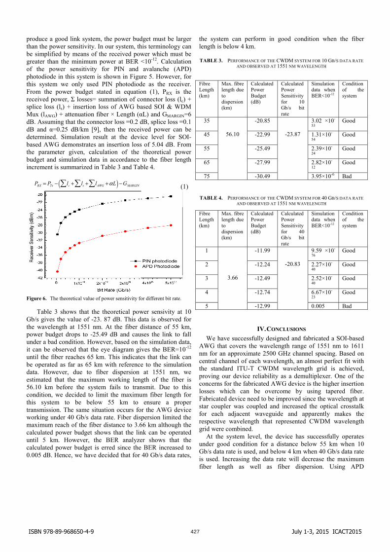
produce a good link system, the power budthan the power sensitivity. In our system, thbe simplified by means of the received powgreater than the minimum power at BER <of the power sensitivity for PIN and photodiode in this system is shown in Figuthis system we only used PIN photodiodFrom the power budget stated in equatioreceived power, losses= summation of cosplice loss (ls) + insertion loss of AWG baMux (lAWG) + attenuation fiber × Length (dB. Assuming that the connector loss =0.2 ddB and =0.25 dB/km [9], then the receidetermined. Simulation result at the devibased AWG demonstrates an insertion lossthe parameter given, calculation of the budget and simulation data in accordance increment is summarized in Table 3 and Tab
PRX = PTx ! lc + ls + lAWG +"L( ) !GMARGIN
Figure 6. The theoretical value of power sensitivity fo
Table 3 shows that the theoretical powGb/s gives the value of -23. 87 dB. This dthe wavelength at 1551 nm. At the fiber dpower budget drops to -25.49 dB and cauunder a bad condition. However, based on tit can be observed that the eye diagram giuntil the fiber reaches 65 km. This indicatebe operated as far as 65 km with referencedata. However, due to fiber dispersion estimated that the maximum working leng56.10 km before the system fails to trancondition, we decided to limit the maximuthis system to be below 55 km to transmission. The same situation occurs foworking under 40 Gb/s data rate. Fiber dispmaximum reach of the fiber distance to 3.6calculated power budget shows that the linuntil 5 km. However, the BER analyzecalculated power budget is erred since the0.005 dB. Hence, we have decided that for
dget must be larger his terminology can wer which must be <10-12. Calculation avalanche (APD)
ure 5. However, for de as the receiver. on (1), PRX is the onnector loss (lc) + ased SOI & WDM L) and GMARGIN=6
dB, splice loss =0.1 ived power can be ice level for SOI-s of 5.04 dB. From
theoretical power to the fiber length
ble 4.
(1)
or different bit rate.
wer sensivity at 10 data is observed for distance of 55 km,
uses the link to fall the simulation data, ves the BER=10-12 es that the link can e to the simulation at 1551 nm, we
gth of the fiber is nsmit. Due to this um fiber length for
ensure a proper or the AWG device persion limited the
66 km although the nk can be operated er shows that the BER increased to 40 Gb/s data rates,
the system can perform in golength is below 4 km.
TABLE 3. PERFORMANCE OF THE CWAND OBSERVED AT 15
Fibre Length (km)
Max. fibre length due to dispersion (km)
Calculated Power Budget (dB)
CPSfGr
35
56.10
-20.85
45 -22.99
55 -25.49
65 -27.99
75 -30.49
TABLE 4. PERFORMANCE OF THE CWAND OBSERVED AT 15
Fibre Length (km)
Max. fibre length due to dispersion (km)
Calculated Power Budget (dB)
CPSfGr
1
3.66
-11.99
2 -12.24
3 -12.49
4 -12.74
5 -12.99
IV. CONC
We have successfully designAWG that covers the wavelengnm for an approximate 2500 Gcentral channel of each wavelenthe standard ITU-T CWDM proving our device reliability aconcerns for the fabricated AWGlosses which can be overcoFabricated device need to be imstar coupler was coupled and for each adjacent waveguiderespective wavelength that repgrid were combined.
At the system level, the devunder good condition for a disGb/s data rate is used, and belowis used. Increasing the data ratfiber length as well as fib
ood condition when the fiber
WDM SYSTEM FOR 10 GB/S DATA RATE 51 NM WAVELENGTH
Calculated Power Sensitivity for 10 Gb/s bit rate
Simulation data when BER<10-12
Condition of the system
-23.87
3.02 ×10-
53 Good
1.31×10-
54 Good
2.39×10-
24 Good
2.82×10-
12 Good
3.95×10⁻⁶ Bad
WDM SYSTEM FOR 40 GB/S DATA RATE 51 NM WAVELENGTH
Calculated Power Sensitivity for 40 Gb/s bit rate
Simulation data when BER<10-12
Condition of the system
-20.83
9.59 ×10-
76 Good
2.27×10-
40 Good
2.52×10-
40 Good
6.67×10-
23 Good
0.005 Bad
CLUSIONS ned and fabricated a SOI-based gth range of 1551 nm to 1611
GHz channel spacing. Based on ngth, an almost perfect fit with wavelength grid is achieved,
as a demultiplexer. One of the G device is the higher insertion
ome by using tapered fiber. mproved since the wavelength at
increased the optical crosstalk e and apparently makes the presented CWDM wavelength
vice has successfully operates stance below 55 km when 10 w 4 km when 40 Gb/s data rate te will decrease the maximum ber dispersion. Using APD
427ISBN 978-89-968650-4-9 July 1-3, 2015 ICACT2015

photodiode and dispersion shifted fibre (DSF) will possibly increase the maximum fiber reach and improve the whole system.
ACKNOWLEDGMENT This work has been filed for patent by Universiti
Kebangsaan Malaysia (UKM) under filing No: UKM3.2.29/108/2/741 and is supported by the Malaysian Ministry of Education under the research grant FRGS/2/2013/SG02/UKM/02/4.
REFERENCES [1] J. Zou, X. Xia, G. Chen, T. Lang, and J-J. He, �“Birefringence
compensated silicon nanowire arrayed waveguide grating for CWDM Optical Interconnects�”, Optics Lett., vol. 39, no.7, pp. 1834-1837, Apr. 2014.
[2] H. Nishi, T. Tsuchizawa, R. Kou, H. Shinojima, T. Yamada, H. Kimura, Y. Ishikawa, K. Wada, and K. Yamada, �“Monolithic integration of a silica AWG and Ge photodiodes on Si photonic platform for one-chip WDM receiver.,�” Opt. Express, vol. 20, no. 8, pp. 9312�–21, Apr. 2012.
[3] X. Chen, C. Li, and H. K. Tsang, �“Device engineering for silicon photonics,�” NPG Asia Mater. 3(1), 34�–40, (2011).
[4] S. Pathak, M. Vanslembrouck, P. Dumon, D. Van Thourhout, and W. Bogaerts, �“Compact SOI-based polarization diversity wavelength de-multiplexer circuit using two symmetric AWGs.,�” Opt. Express, vol. 20, no. 26, pp. B493�–500, Dec. 2012.
[5] Q. Fang, F. Li, and Y. Liu, �“Compact SOI arrayed waveguide grating demultiplexer with broad spectral response,�” Opt. Commun., vol. 258, no. 2, pp. 155�–158, Feb. 2006.
[6] N. Juhari, P. S. Menon, A. A. Ehsan, and S. Shaari, �“Optical loss analysis in 13-channel SOI-based AWG for CWDM network,�” J. Nonlinear Opt. Phys. Mater. Vol 23, no.1, pp. 1450008, 2014.
[7] N. Juhari, P.S. Menon and A.A. Ehsan, �“12-channel Tapered SOI-based AWG for CWDM System�” in Proc. 4th International Conf. on Photonics ICP, pp. 230-233, IEEE, Malaysia (2013).
[8] N. Juhari, P. S. Menon, A. A. Ehsan, and S. Shaari, �“Optimal design of linear tapered double S-shaped arrayed waveguide grating for broad channel spacing on silicon-on-insulator�”, Opt. Eng., vol. 53 no. 8, pp. 087110, August 2014.
[9] International Telecommunication Union ITU-T 2009 Manual, Optical Fibres, Cables and Systems.
Nurjuliana Juhari obtained her B.Sc and M.Sc from University of Malaya (UM) under the physics department in the years 2003 and 2007. She is currently pursuing a PhD degree at Photonics Technology Laboratory, IMEN, UKM. Her research interests revolve around the design, fabrication and characterization of passive devices in sub-micron level SOI based Arrayed Waveguide Grating (AWG) for the application in CWDM system.
P Susthitha Menon (M�’09) received her B.Eng. degree in Electrical, Electronics and System Engineering from The National University of Malaysia (Universiti Kebangsaan Malaysia - UKM) in 1999 and the M.Sc. degree in optoelectronics from UKM in 2005. She obtained a Ph.D. degree with distinction in Optoelectronics and Nanophotonics from the Institute of Microengineering and Nanoelectronics (IMEN), UKM in 2008. She is currently a senior research fellow at IMEN and her current research interests are in the field of nanophotonic optical waveguides, surface plasmon resonance (SPR), optoelectronics and optical fiber based sensors, which are all geared towards bio-sensing.
Abang Annuar Ehsan received a B.E. degree in Electrical Engineering from University of New South Wales, Australia in 1996, and a M.Sc. degree in Microelectronics from UKM, in 2002. He received a Ph.D degree in Applied
Science from Universiti Teknologi MARA, Malaysia in 2010 and a Ph.D in Microengineering and Nanoelectronics from UKM, in 2012. His research interests include plastic optical fiber devices, planar optical waveguides, optical design and modeling, and rapid manufacturing of optical devices. Sahbudin Shaari received the M.Sc degree (Quantum Electronics) from University of Essex and Ph.D degree (Microelectronics) from University of Wales in 1980 and 1989 respectively. From 1978 to 2003 he was a lecturer at the Department of Electrical, Electronics and System Engineering, UKM. In 1982, he introduced optical fiber communications into the country. He became a full-fledged professor in microelectronics/photonics in 2002. In 2003, he joined IMEN, UKM as the head of Photonics and Nanophotonics Research Group. Currently his research interest is in the field of silicon photonics.
428ISBN 978-89-968650-4-9 July 1-3, 2015 ICACT2015