doe study of epitaxial layer thickness and resistivity ... · diode 2d structure and electrical...
TRANSCRIPT
24
Original scientific paper
MIDEM Society
DOE Study of Epitaxial Layer Thickness and Resistivity Effects on P-i-N Diode for beyond 300 V of Reverse Voltage ApplicationsJ. H. See1, M. K. Md Arshad1,2, M. F. M. Fathil1, C. H Voon1, U. Hashim1,2, Subash C. B. Gopinath1
1Institute of Nano Electronic Engineering, Universiti Malaysia Perlis, Kangar, Perlis, Malaysia2School of Microelectronic Engineering, Universiti Malaysia Perlis, Kangar, Perlis, Malaysia
Abstract: A discrete power switching device used in the applications of computer and telecommunications requires operating less than 300 V during reverse bias, but for the use of motor control, robotics, and power distribution, it requires operating at beyond 300 V. With the current design structure, the P-i-N diode device can only operate at 250 V. To widen the operating range of the P-i-N power switching avalanche diode that can be operated more than 300 V, we studied the effects of the epitaxial layer thickness (WD) and resistivity (ρ) during forward and reverse biasing by performing a process simulation as well as the confirmation on the two level factorials of design of experiment (DOE) of physical wafers. The result shows that, the changes of the WD of 42 µm and ρ of 32 ohm·cm on a P-i-N diode can increase the reverse breakdown voltage (VR) performance beyond 300 V during reverse bias.
Keywords: Forward voltage; Breakdown voltage; Power device
Načrtovanje eksperimenta vplivov debeline in upornosti epitaksijske plasti P-i-N diode pri reverznih napetostih nad 300 VIzvleček: Diskretni močnostni stikalni element za uporabo v računalnikih in telekomunikacijah zahteva delovanja pri zaporni napetosti pod 300 V. Pri krmiljenju motorjev, v robotiki ali pri močnostnih aplikacijah pa zahteva delovanje v zaporni smeri preko 300 V. Trenutna struktura P-i-N diode lahko deluje le do 250. Za višje napetosti je potrebna močnostna plazovita P-i-N dioda, na kateri smo preučevali vplive debeline epitaksijske plasti in upornosti pri prevodni in zaporni napetosti. Analiza sloni na simulaciji procesa dvonivojske faktorizacije načrtovanja eksperimenta silicijeve rezine. Rezultati izkazujejo, da sprememba debeline za 42 µm in upornosti za 32 ohm·cm zviša prebojno napetost preko 300 V.
Ključne besede: Forward voltage; Breakdown voltage; Power device
* Corresponding Author’s e-mail: [email protected]
Journal of Microelectronics, Electronic Components and MaterialsVol. 47, No. 1(2017), 24 – 31
1 Introduction
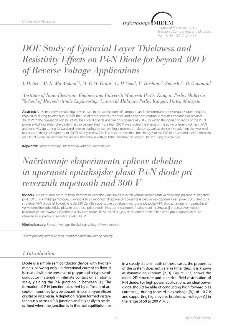
Diode is a simple semiconductor device with two ter-minals, allowing only unidirectional current to flow. It is created with the presence of p-type and n-type semi-conductor materials in intimate contact on an atomic scale, yielding the P-N junction in between [1]. The formation of P-N junction occurred by diffusion of ac-ceptor impurities (p-type dopant) into an n-type silicon crystal or vice versa. A depletion region formed instan-taneously across a P-N junction and it is easily to be de-scribed when the junction is in thermal equilibrium or
in a steady state: in both of these cases, the properties of the system does not vary in time; thus, it is known as dynamic equilibrium [2, 3]. Figure 1 (a) shows the diode 2D structure and electrical field distribution of P-N diode. For high power applications, an ideal power diode should be able of conducting high forward bias current (IF) during forward bias voltage (VF) of ~0.7 V and supporting high reverse breakdown voltage (VR) in the range of 50 to 200 V [4, 5].
25
J.H. See1 et al; Informacije Midem, Vol. 47, No. 1(2017), 24 – 31
During reverse bias, P-N diode experiences the ava-lanche breakdown. To achieve the avalanching, besides the requirement of a large field, it also requires a suffi-cient distance to allow the electron to accelerate, hence gain enough kinetic energy, and lead to an avalanche of multiple hole-electron pair’s creation [6]. In other words, to ensure the high VR, a thick n-type substrate bulk is required for a vertical structure of simple P-N junction diode. For a vertical structure of P-N junction diode, a very thick wafer substrate bulk can be used to fulfill the requirement of a power diode. However, thicker substrate exhibits several drawbacks, which are 1) greater weight and 2) higher production cost.
Alternatively, higher VR and IF can be achieved by using the P-i-N diode structure with a thinner substrate. The P-i-N diode was one of the very first semiconductor de-vices developed for power circuit application [4, 7]. This evolution came from a conventional P-N junction di-ode with the addition of an extra intrinsic layer depos-ited between p-type and n-type regions. Figure 1 (b) (i) illustrates the P-i-N diode structure in 2D structure and electrical field distribution of P-i-N diode. In P-i-N diode, the reverse breakdown voltage is dependence on the depletion region formed with a P-N junction structure. The voltage is primary determined within the N-type drift region. Thus low doping concentration for the N-type drift region is more beneficial in order to hold the carrier from flowing between P- and N-region. The sili-con P-i-N diode is designed to support large voltages, which rely upon the high level injection of minority carrier in the N-type drift region [8]. Therefore, to sup-port a large voltage in the reverse breakdown voltage mode, an appropriate choice of doping concentration and thickness of the N-drift region needs to be made. Nevertheless, a narrower drift region is preferable be-cause it can contain smaller amount of stored charges during the on-state operation, enabling faster turn-off.
Material substitution is one way to achieve narrower drift region thickness [9]. For example, by using silicon carbide, narrower drift region can be attained when compared to silicon devices. This is due to much larger electric field can be supported in silicon carbide. As a result, it favors a faster switching speed with reduced reverse recovery current and very high breakdown voltage can be achieved [10]. However, the high cost is a major concern, and silicon P-i-N diode still can be modified and continue to play an important role in the application, especially in medium range of breakdown voltage.
This can be explained based on expression as shown in Equation (2). The expression for VR in this P-i-N diode can be derived by using higher critical electric field (EC) [11, 12] Based on Figure 1 (b) (ii), EC is the critical elec-
tric field and WD is depletion region thickness during reverse bias. Since P-i-N diode operates in a thickness-limited mode, which is controlled by the thickness of N- region epitaxial layer, the WD can be referred to as the thickness of the N- epitaxial layer in i-region. The VR can be calculated as the area of the trapezium (Figure 1 (b) (ii)) as in Equation (2).
( )11 2R C DV E E W= + (2)
By using the Equation (2) for the variation in the electric field with distance:
1
DC D
S
q NE E W= −∈
(3)
and substituting Equation (3) in Equation (2), the VR for the punch through diode is obtained as in Equation (4):
2 2D D
R C DS
q N WV E W= −∈
(4)
The VR can be affected by the variable thickness of the N- region (WD) and the doping concentration of the N-
Figure 1: Comparison of ideal (a) P-N junction and (b) P-i-N diode in terms of (i) 2D structure and (ii)electrical field distribution.
26
epitaxial layer (ND). The ND can be translated into the resistivity of the N- layer [11],. The increase of the ND results in lower resistivity.
In this paper, P-i-N diode with high resistivity N region (N- region) is used to replace the intrinsic layer. For this purpose, a commercially available 250 V P-i-N power switching diode was used to evaluate effects of N- epi-taxial layer thickness (WD) and resistivity (ρ) as the in-trinsic layer effect to the P-i-N power switching diode on the performance of current-voltage (I-V) charac-teristic in terms of diode’s VR. The aim of this study is to have a diode that can withstand beyond 250 V for motor control, robotics and power distribution appli-cations. The N- region is deposited on top of the wafer substrate through epitaxial process.
2 Methodology
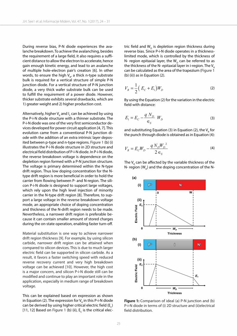
In this work, the simulation of the P-i-N diode is per-formed using technology computer-aided design (TCAD) simulation software i.e. Sentaurus WorkBench, as well as the fabrication and characterization of the P-i-N diode. The P-i-N power switching diode diffuses a circular shaped boron (P+ anode junction) into an N- type epitaxial layer on a low bulk resistance N+ substrate. Another N+ diffused isolation region at the perimeter of the anode junction to reduces leakage current. The backside of the wafer is sputtered with platinum (Pt) and gold (Au). The process followed by a quick drive-in cycle for both elements, from the bulk all the way through the epitaxial layer and the P+ anode junction. Pt improves the life time cycle, reducing the reverse recovery time (trr) [13]. Au increases the epitax-ial layer’s trr resistance, which increases the resistance of drastic oscillation of the signal. Thus, it produces a wider P-N junction depletion region and reducing the capacitance. Figure 2 illustrates the cross-section de-sign of the P-i-N power switching diode.
Figure 2: Cross-section structure of P-i-N power switch-ing diode.
2.1 Numerical Simulation
The VR of P-i-N power switching diode operates in WD limited mode of the epitaxial layer. The first approach
is to alter the WD by adjusting the depth of the P+ an-ode junction through diffusion with boron as demon-strated in Figure 2. By reducing the junction diffusion drive time, a shallower anode junction is formed. With this approach, the WD is increased [14]. However, this method has several weaknesses. The anode junction diffusion process is difficult to control, which leads to process variation. The inconsistent process tempera-ture of diffusion furnace results in lower VR at the edges compared to the centre of the wafers, as wafer edges tend to have a higher process temperature compared to the wafer centre [14]. Another drawback is the dif-fusion process is performed under a high temperature, thus caused the up diffusion from the heavily doped N+ bulk substrate. This resulted in a less favourable higher VF [14].
The second approach is to adjust the epitaxial layer pro-file (WD and ρ) of the substrate [14]. With the zero punch through structure of the P-i-N diode, as observed from the Equation (4), the WD and ND are dominant factors, which increase the VR. The second approach is more favourable due to better control of wafer fabrication process.
A series of simulation and DOE is performed to show the effects of the WD and ND on the I-V characteristic using TCAD simulation software. The applications of TCAD simulation include technology and design rule development, as well as the extraction of compact models for manufacturability [15]. Initially, a half diode cross-section structure is designed by using SProcess. After the half diode is created, reflecting boundary con-ditions is applied to generate a full simulation diode model symmetrically.
For the SProcess step, a layer of phosphorus dopant (N- epitaxial) thickness is grown on top of the N+ bulk silicon substrate, which is initially doped with arsenic. The silicon substrate orientation of <100> is used. The dopant parameter is defined as @epidose@ and WD pa-rameter is defined as @epiThick@. With the parameters are defined in general, several WD and doping concen-trations are utilized in the simulation (Table 1) to evalu-ate the output response of the I-V characteristic.
Table 1: Simulation thickness and concentration dos-age of N- layer.
Split Epitaxial Layer Thickness,
@epiThick@ (µm)
Epitaxial Layer Dopant Concentration,
@epidose@ (cm-3)a 42 1.68×10¹⁴
b 42 1.58×10¹⁴
c 42 1.48×10¹⁴
d 42 1.36×10¹⁴
J.H. See1 et al; Informacije Midem, Vol. 47, No. 1(2017), 24 – 31
27
e 34 1.68×10¹⁴
f 34 1.58×10¹⁴
g 34 1.48×10¹⁴
h 34 1.36×10¹⁴
The selection of the 34 µm and 42 µm thickness of WD in simulation is due to lower and upper specification on the existing diode device epitaxial layer evaluation shown as group C in Figure 5, which will be explained in Section 2.2. The various dopant concentrations of N- epitaxial layer are selected to measure the electrical output response impact in simulation. By adjusting the phosphorus dopant concentration at the N- epitaxy layer via implantation, the ρ can be controlled, since the dopant concentration is inversely proportional with resistivity [16].
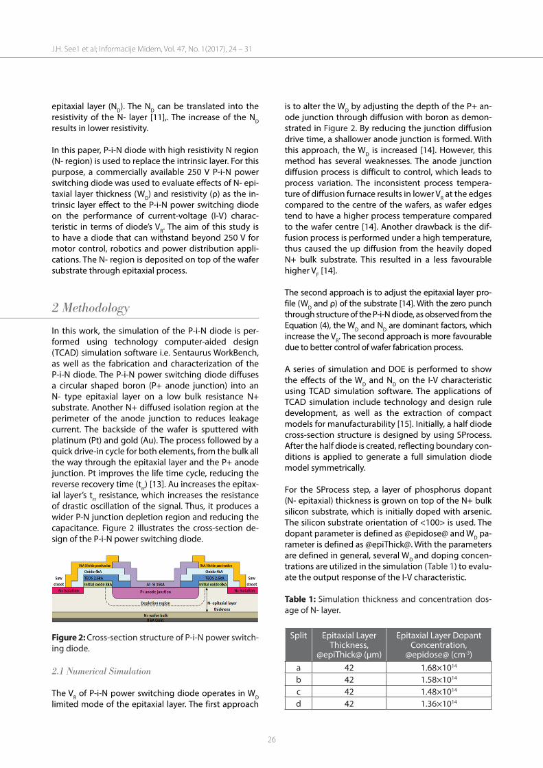
Subsequently, a 1 µm thickness of oxide layer is depos-ited, followed by opening of the anode area with the photolithography and etching process for electrode deposition. Next, boron is implanted with a dosage of 5×1015 cm-3, anode junction drive in temperature and time for 1200 °C and 240 mins, respectively. After the anode junction is formed, the oxide layer is stripped off and then re-deposited with the same thickness. This re-deposited oxide layer is to react as the pattern oxide, followed by a 2 µm thickness of front metal Al layer, which act as the ohmic contact and a 1 µm thickness of Si3N4 nitride layer, which act as the passivation layer. All of these three layers are formed with photolithog-raphy and etching process. The final device structure is shown in Figure 3.
Figure 3: P-i-N diode structure with doping profile dis-tribution.
2.2 Design of experiment and process split
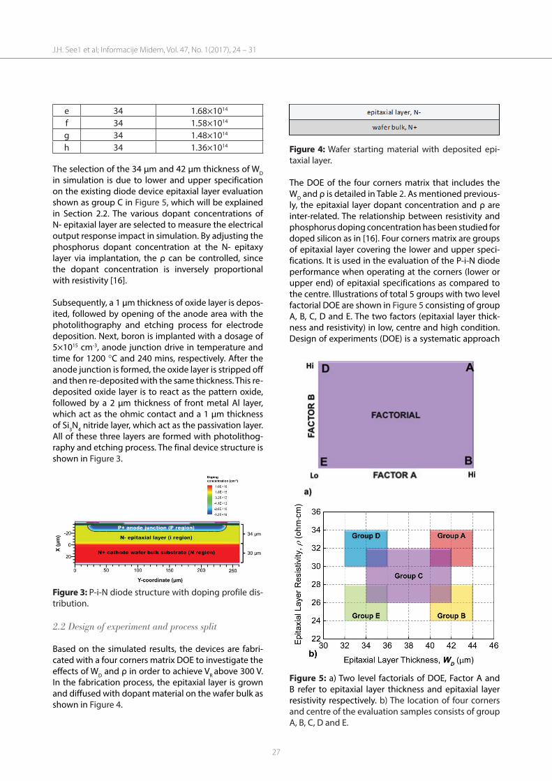
Based on the simulated results, the devices are fabri-cated with a four corners matrix DOE to investigate the effects of WD and ρ in order to achieve VR above 300 V. In the fabrication process, the epitaxial layer is grown and diffused with dopant material on the wafer bulk as shown in Figure 4.
Figure 4: Wafer starting material with deposited epi-taxial layer.
The DOE of the four corners matrix that includes the WD and ρ is detailed in Table 2. As mentioned previous-ly, the epitaxial layer dopant concentration and ρ are inter-related. The relationship between resistivity and phosphorus doping concentration has been studied for doped silicon as in [16]. Four corners matrix are groups of epitaxial layer covering the lower and upper speci-fications. It is used in the evaluation of the P-i-N diode performance when operating at the corners (lower or upper end) of epitaxial specifications as compared to the centre. Illustrations of total 5 groups with two level factorial DOE are shown in Figure 5 consisting of group A, B, C, D and E. The two factors (epitaxial layer thick-ness and resistivity) in low, centre and high condition. Design of experiments (DOE) is a systematic approach
Figure 5: a) Two level factorials of DOE, Factor A and B refer to epitaxial layer thickness and epitaxial layer resistivity respectively. b) The location of four corners and centre of the evaluation samples consists of group A, B, C, D and E.
J.H. See1 et al; Informacije Midem, Vol. 47, No. 1(2017), 24 – 31
28
in engineering problem-solving that applies principles and techniques from the data collection stage. The out-put response from the data collection includes forward voltage, reverse breakdown voltage and reverse leak-age current. The focus on the study is to increase the VR during reverse bias without changing much of the VF and IR.
A total of 15 wafers lot are fabricated with the same P-i-N diode design at process corners with low/high WD and low/high ρ. Afterward, the wafers are fabricated and electrically characterized. Electrical results of VF, VR, and reverse leakage current (IR) are the main param-eters of interest and then analysed with statistical soft-ware (for profiler study). The predicted profiler study is done to determine the dominant factor that affects the electrical performance and the optimal epitaxial pro-file. To ensure the repeatability of the result, each of the splits is repeated 3 times for the wafer fabrication and characterization.
3 Results and discussions
3.1 Simulation results
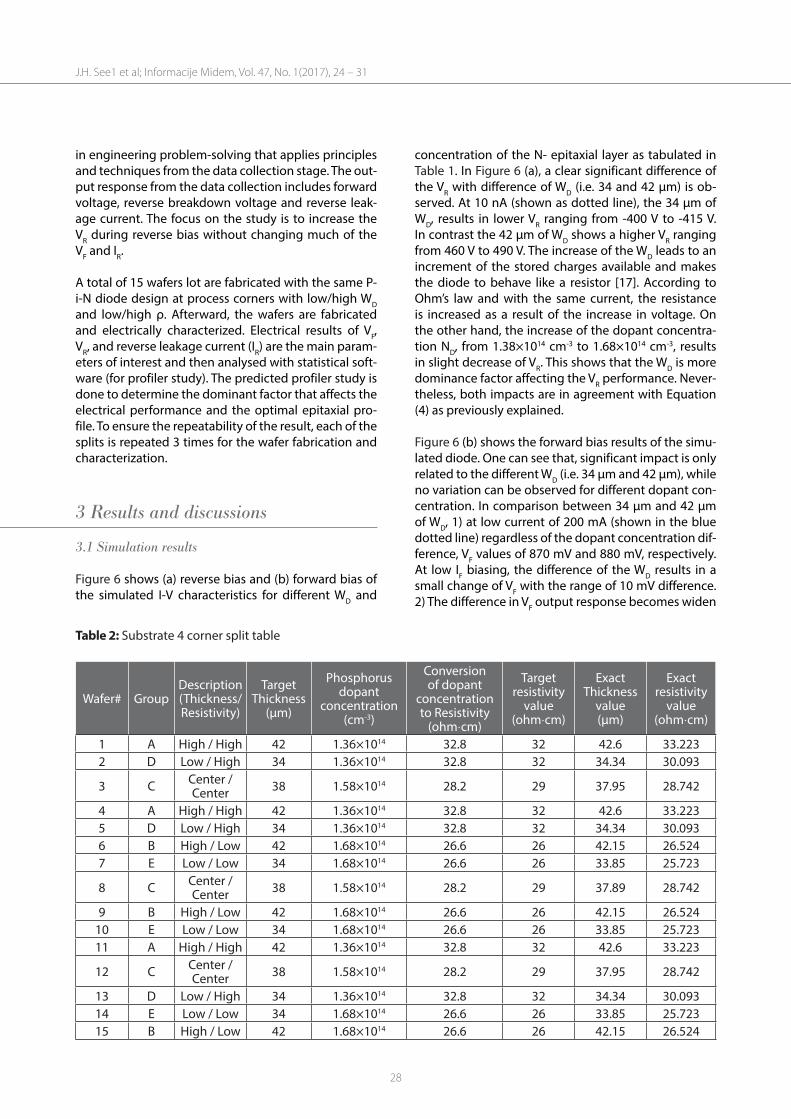
Figure 6 shows (a) reverse bias and (b) forward bias of the simulated I-V characteristics for different WD and
concentration of the N- epitaxial layer as tabulated in Table 1. In Figure 6 (a), a clear significant difference of the VR with difference of WD (i.e. 34 and 42 µm) is ob-served. At 10 nA (shown as dotted line), the 34 µm of WD, results in lower VR ranging from -400 V to -415 V. In contrast the 42 µm of WD shows a higher VR ranging from 460 V to 490 V. The increase of the WD leads to an increment of the stored charges available and makes the diode to behave like a resistor [17]. According to Ohm’s law and with the same current, the resistance is increased as a result of the increase in voltage. On the other hand, the increase of the dopant concentra-tion ND, from 1.38×1014 cm-3 to 1.68×1014 cm-3, results in slight decrease of VR. This shows that the WD is more dominance factor affecting the VR performance. Never-theless, both impacts are in agreement with Equation (4) as previously explained.
Figure 6 (b) shows the forward bias results of the simu-lated diode. One can see that, significant impact is only related to the different WD (i.e. 34 µm and 42 µm), while no variation can be observed for different dopant con-centration. In comparison between 34 µm and 42 µm of WD, 1) at low current of 200 mA (shown in the blue dotted line) regardless of the dopant concentration dif-ference, VF values of 870 mV and 880 mV, respectively. At low IF biasing, the difference of the WD results in a small change of VF with the range of 10 mV difference. 2) The difference in VF output response becomes widen
Table 2: Substrate 4 corner split table
Wafer# GroupDescription (Thickness/ Resistivity)
Target Thickness
(µm)
Phosphorus dopant
concentration (cm-3)
Conversion of dopant
concentration to Resistivity
(ohm⋅cm)
Target resistivity
value (ohm⋅cm)
Exact Thickness
value (µm)
Exact resistivity
value (ohm⋅cm)
1 A High / High 42 1.36×10¹⁴ 32.8 32 42.6 33.2232 D Low / High 34 1.36×10¹⁴ 32.8 32 34.34 30.093
3 C Center / Center 38 1.58×10¹⁴ 28.2 29 37.95 28.742
4 A High / High 42 1.36×10¹⁴ 32.8 32 42.6 33.2235 D Low / High 34 1.36×10¹⁴ 32.8 32 34.34 30.0936 B High / Low 42 1.68×10¹⁴ 26.6 26 42.15 26.5247 E Low / Low 34 1.68×10¹⁴ 26.6 26 33.85 25.723
8 C Center / Center 38 1.58×10¹⁴ 28.2 29 37.89 28.742
9 B High / Low 42 1.68×10¹⁴ 26.6 26 42.15 26.52410 E Low / Low 34 1.68×10¹⁴ 26.6 26 33.85 25.72311 A High / High 42 1.36×10¹⁴ 32.8 32 42.6 33.223
12 C Center / Center 38 1.58×10¹⁴ 28.2 29 37.95 28.742
13 D Low / High 34 1.36×10¹⁴ 32.8 32 34.34 30.09314 E Low / Low 34 1.68×10¹⁴ 26.6 26 33.85 25.72315 B High / Low 42 1.68×10¹⁴ 26.6 26 42.15 26.524
J.H. See1 et al; Informacije Midem, Vol. 47, No. 1(2017), 24 – 31
29
between various WD with the increase of the IF. This can be explained, when a P-i-N diode is forward biased, where holes and electrons are injected from the P and N regions into the i-region, which is represented as WD. These charges do not recombine immediately. Instead, a finite quantity of charge always remains stored and results in a lowering of the ρ. So, the increase of IF leads the decrease of the forward series resistance (RS) [18]. The WD plays a greater role to change the VF with low resistivity.
(a)
(b)Figure 6: I-V characteristics under (a) reverse bias and (b) forward bias for different WD and dopant concentra-tions.
From the simulation, by changing the WD and dopant concentration of the epitaxial layer, the VR shows more significant difference compared to VF. The reason being the P-i-N diode exhibiting reverse capacitance charac-teristics during reverse bias where dopant concentra-tion and the WD shows a more responsive curve. While forward biasing, P-i-N diode exhibits the forward se-ries resistance characteristics where the difference of the WD plays a greater role when the IF is increased to a certain level [18], [19]. The phenomenon of the less responsive output on the forward bias is preferable as the focus on the study is to increase the VR during re-verse bias without changing the VF.
With the confirmation of the theory through the TCAD simulation software, a wafer fabrication DOE has been conducted to validate the results by taking into ac-count of the process variation and material variation.
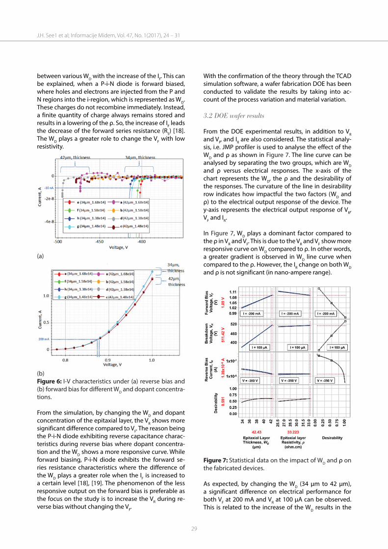
3.2 DOE wafer results
From the DOE experimental results, in addition to VR and VF, and IR are also considered. The statistical analy-sis, i.e. JMP profiler is used to analyse the effect of the WD and ρ as shown in Figure 7. The line curve can be analysed by separating the two groups, which are WD and ρ versus electrical responses. The x-axis of the chart represents the WD, the ρ and the desirability of the responses. The curvature of the line in desirability row indicates how impactful the two factors (WD and ρ) to the electrical output response of the device. The y-axis represents the electrical output response of VR, VF and IR.
In Figure 7, WD plays a dominant factor compared to the ρ in VR and VF. This is due to the VR and VF show more responsive curve on WD compared to ρ. In other words, a greater gradient is observed in WD line curve when compared to the ρ. However, the IR change on both WD and ρ is not significant (in nano-ampere range).
Figure 7: Statistical data on the impact of WD and ρ on the fabricated devices.
As expected, by changing the WD (34 µm to 42 µm), a significant difference on electrical performance for both VF at 200 mA and VR at 100 µA can be observed. This is related to the increase of the WD results in the
J.H. See1 et al; Informacije Midem, Vol. 47, No. 1(2017), 24 – 31
30
VR and VF is also increased. Interesting to note that, an increase of VF around 10 mV can be observed in Figure 7, is similar to the result obtained in simulation Figure 6 (b). With WD increased from 34 µm to 42 µm, at 100 µA, the VR shows almost similar response between simula-tions versus actual DOE. The voltage different between simulation and actual DOE is around 20 V is due to the uniformity of the boron pre deposition process.
In Figure 7, based on the statistical analysis JMP soft-ware, the VR shows a significant improvement from 300 V to more than 500 V when replaced with WD of 42.43 µm and the ρ of 33.22 ohm.cm.
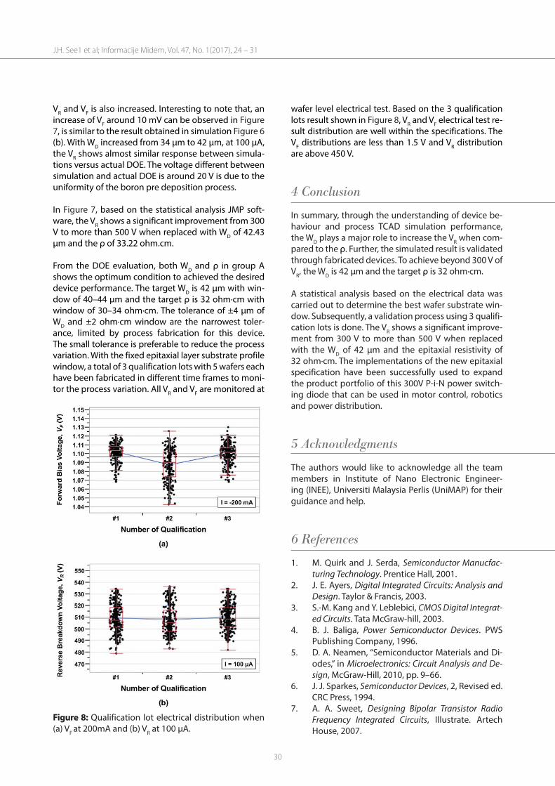
From the DOE evaluation, both WD and ρ in group A shows the optimum condition to achieved the desired device performance. The target WD is 42 µm with win-dow of 40–44 µm and the target ρ is 32 ohm·cm with window of 30–34 ohm·cm. The tolerance of ±4 µm of WD and ±2 ohm·cm window are the narrowest toler-ance, limited by process fabrication for this device. The small tolerance is preferable to reduce the process variation. With the fixed epitaxial layer substrate profile window, a total of 3 qualification lots with 5 wafers each have been fabricated in different time frames to moni-tor the process variation. All VR and VF are monitored at
wafer level electrical test. Based on the 3 qualification lots result shown in Figure 8, VR and VF electrical test re-sult distribution are well within the specifications. The VF distributions are less than 1.5 V and VR distribution are above 450 V.
4 Conclusion
In summary, through the understanding of device be-haviour and process TCAD simulation performance, the WD plays a major role to increase the VR when com-pared to the ρ. Further, the simulated result is validated through fabricated devices. To achieve beyond 300 V of VR, the WD is 42 µm and the target ρ is 32 ohm·cm.
A statistical analysis based on the electrical data was carried out to determine the best wafer substrate win-dow. Subsequently, a validation process using 3 qualifi-cation lots is done. The VR shows a significant improve-ment from 300 V to more than 500 V when replaced with the WD of 42 µm and the epitaxial resistivity of 32 ohm·cm. The implementations of the new epitaxial specification have been successfully used to expand the product portfolio of this 300V P-i-N power switch-ing diode that can be used in motor control, robotics and power distribution.
5 Acknowledgments
The authors would like to acknowledge all the team members in Institute of Nano Electronic Engineer-ing (INEE), Universiti Malaysia Perlis (UniMAP) for their guidance and help.
6 References
1. M. Quirk and J. Serda, Semiconductor Manucfac-turing Technology. Prentice Hall, 2001.
2. J. E. Ayers, Digital Integrated Circuits: Analysis and Design. Taylor & Francis, 2003.
3. S.-M. Kang and Y. Leblebici, CMOS Digital Integrat-ed Circuits. Tata McGraw-hill, 2003.
4. B. J. Baliga, Power Semiconductor Devices. PWS Publishing Company, 1996.
5. D. A. Neamen, “Semiconductor Materials and Di-odes,” in Microelectronics: Circuit Analysis and De-sign, McGraw-Hill, 2010, pp. 9–66.
6. J. J. Sparkes, Semiconductor Devices, 2, Revised ed. CRC Press, 1994.
7. A. A. Sweet, Designing Bipolar Transistor Radio Frequency Integrated Circuits, Illustrate. Artech House, 2007.
Figure 8: Qualification lot electrical distribution when (a) VF at 200mA and (b) VR at 100 µA.
J.H. See1 et al; Informacije Midem, Vol. 47, No. 1(2017), 24 – 31
31
8. J. F. White, Microwave Semiconductor Engineer-ing, Illustrate. Springer Science & Business Media, 2012.
9. Z. Xu et al., “Fully- and Quasi-Vertical GaN-on-Si p-i-n Diodes: High Performance and Comprehen-sive Comparison,” IEEE Trans. Electron Devices, pp. 1–7, 2017.
10. J. Xu, “Technology for Planar Power Semiconduc-tor Devices Package with Improved Voltage Rat-ing Technology for Planar Power Semiconductor Devices Package with Improved Voltage Rating,” Virginia Polytechnic Institute and State University, 2008.
11. B. Jayant Baliga, Fundamental of Power Semicon-ductor Devices. Springer, 2008.
12. P. Spirito, Power Semiconductor Devices. Dept of Electronics and Telecommunications, University Federico II.
13. C. M. Cheh et al., “The Impacts of Platinum Diffu-sion to the Reverse Recovery Lifetime of a High Power Diode Devices,” MATEC Web Conf., vol. 78, p. 1089, Oct. 2016.
14. C. C. Mee, M. K. Md Arshad, M. Fathil, and U. Hashim, “The effects of intrinsic silicon epitaxial layer in p-i-n diode for high power devices,” ARPN J. Eng. Appl. Sci., vol. 10, no. 18, 2015.
15. R. W. Dutton and A. J. Strojwas, “Perspectives on technology and technology-driven CAD,” IEEE Trans. Comput. Des. Integr. Circuits Syst., vol. 19, no. 12, pp. 1544–1560, 2000.
16. J. C. Irvin, “Resistivity of bulk silicon and of dif-fused layers in silicon,” Bell Syst. Tech. J., vol. 41, no. 2, pp. 387–410, 1962.
17. N. I. Shuhaimi et al., “Comparison on I-V perfor-mances of Silicon PIN diode towards width vari-ations,” in 2010 IEEE International Conference on Semiconductor Electronics (ICSE2010), 2010, pp. 12–14.
18. B. Doherty, “PIN Diode Fundamentals,” Microsemi.19. W. E. Doherty and R. D. Joos, The PIN Diode Circuit
Designers’ Handbook. Watertown: Microsemi Cor-poration, 1998.
Arrived: 05. 11. 2016Accepted: 22. 02. 2017
J.H. See1 et al; Informacije Midem, Vol. 47, No. 1(2017), 24 – 31